This thread has been locked.

If you have a related question, please click the "Ask a related question" button in the top right corner. The newly created question will be automatically linked to this question.

TMS320F28386D-Q1: The ADC result jumps about 30LSB (peak-to-peak)

Part Number: TMS320F28386D-Q1
Other Parts Discussed in Thread: TL431, OPA320, REF35

Hi Team,

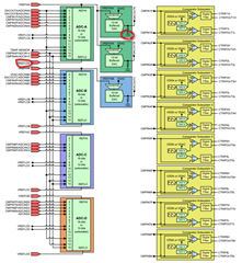
Here're the descriptions of customer's ADC usage:

1. The reference voltage 3V is obtained through TL431, and the test reference voltage ripple Vpp of the oscilloscope is about 3.5mV;

2. Single-ended ADC mode, 12BIT, no post-processing;

3. I have tried setting ACQPS to 15, 64, 240, 500, etc., but there was no improvement;

4. The value of the series resistor Rs between the op amp and C2000 is 100 ohms, and the Cs capacitor has been used with 10nF and 100nF, etc., but there is no improvement;

5. Try the DAC output and test the DAC pin output voltage ripple Vpp about 3mV;

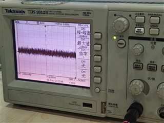
6. When testing the ADC pin value with an oscilloscope, the ripple Vpp is about 5mV;

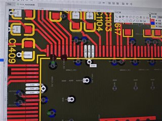
7. VREFLO is connected to AGND on the circuit board;

The ADC input is a 1.5V DC signal (ripple within 5mV). The ADC is used to measure the three phase currents of the frequency converter. It uses a current sensor to convert the AC voltage into a signal with a bias of 1.5V and an amplitude of ±1.2V. The motor has not yet been connected during the debugging stage. Currently only a single ADC input is used.

+++++++++++++++++++++++++++

ADC input circuit:

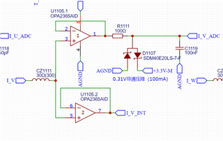
Reference voltage circuit:

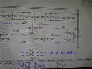
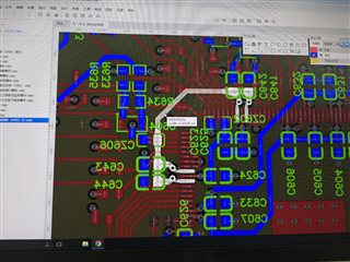
Reference voltage PCB trace:

Reference ground and analog ground are directly connected:

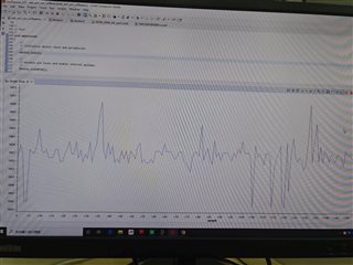
Detected unprocessed ADC value:

ADC pin voltage ripple:

Another question: Will the sampling values obtained by different packages be very different?

--

Thanks & Regards

  • Hello Yale,

    Quick observations about the reference circuit:

    - The capacitance is too much. Does not need more than 22uF

    - Use of an inductive/pi filter is not recommended on voltage reference pins. Because these suppress current fluctuations, they can actually be detrimental to SAR ADC operation which requires fast current transients as internal capacitors are charged and discharged. This may be contributing to the inaccuracy issues.

    Best regards,
    Ibukun

  • Hello Ibukun,

    Thanks for your reply.

    The customer made circuit modifications according to your suggestion. The result is still the same as before, without optimization;
    1) Adjust the capacitance of the Vref pin to 2.2uF, remove the magnetic beads connected in series with the reference voltage, and directly short-circuit the power supply;

    2) Test the ripple of the Vref pin capacitor, which is very low, Vpp is about 3mV.

  • Hello Yale,

    We have seen an issue somewhat similar to this with another customer. In this case there was ground noise coming from a buck converter and ground was routed using traces, so there was a return path from the ADC through the PMIC to the signal source. If this is similar I would consider taking a look at ground routing - particularly with respect to VDDA/VSSA.

    The error spikes seen in the conversion look to be about 2x the ripple amplitude, and since the reference/signal seem to be well-conditioned already, the most likely culprit would seem to be power/ground rail related.

    Best regards,
    Ibukun

  • Hello Ibukun,

    At first, the customer also suspected that it was an analog ground problem, so he tested the VREF reference voltage. The test points were the ground pin of 28386 and the pin of the Vref input chip. The ripple amplitude Vpp is less than 3mV.

    If the grounding is abnormal, this testing method should be able to detect abnormal Vref; or is there any other reliable testing method to verify your statement?

    The current ground connection method is to connect the device reference voltage ground to the device analog ground, and then connect them to AGND on the single board. The DAC output is controlled through the program. The peak-to-peak ripple is within 3mV. Does this mean that the pin grounding is normal? ?

    --

    Thanks & Regards

  • Yale,

    After discussing with our team here, two additional suggestions:

    • Consider moving the overvoltage protection diodes (D1107) to the op amp noninverting input, so that any noise from that network gets filtered.
    • Given that a shunt voltage reference is being used, consider adding an op amp buffer (e.g. OPA320) to help with load regulation. Or alternatively, consider a series voltage reference instead e.g. REF35.

    Best regards,
    Ibukun