This thread has been locked.
If you have a related question, please click the "Ask a related question" button in the top right corner. The newly created question will be automatically linked to this question.
Tool/software:
Greetings,
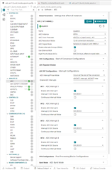
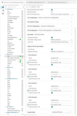
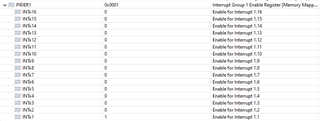
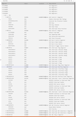
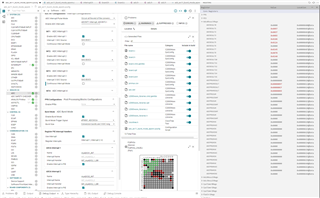
I seperated the round robin wheel into "SOC0 to SOC6" :High Prio (SOC0-SOC5 are used, SOC6 is unused) and "SOC7 to SOC15": Round Robin Low Prio(SOC7-SOC15 are used, 3 times a size 3 burst, rince an repeat).
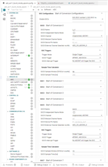
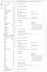
SOC0 to SOC5 are ALL triggered by the ePWM1 ADCSOCA event, RoundRobin-Bust (burstsize = 3) is also triggered by the same ePWM1 ADCSOCA event.
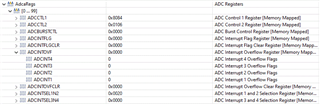
4 ADC IRQs are generated: ADC INT1 at EOC of SOC1 (for test purpose only), ADC INT2 at EOC of SOC3 (for test purpose only), ADC INT3 at EOC of SOC5 (IRQ which im primarily interested in),
ADC INT4 at EOC of SOC15 (for test purpose only)
To my question:
Im quite puzzled, because I thought the IRQs: ADC INT1, ADC INT2, ADC INT3 are always raised and my ISR is always executed at that moment the SOC EOC events are happening.
Debugging should show me something like. Download+Debug, I press start, ADC INT1 happens, ISR is called, breakpoint is hit, core is stopped and only ADCRESULT0 and ADCRESULT1 has a value other than 0x0000,
But debugging seems to show, that at that moment I finally enter the ISR for ther first time all values "SOC0 to SOC5" and "SOC7 to SOC9" are already acquired (ADCRESULT0 to ADCRESULT5 and ADCRESULT7 to ADCRESULT9 have values other than 0x0000).
What I want: ePWM1 ADCSOCA event appears an triggers HighPrio-SOCs and RR-Burst --> HighPrio-SOCs come first --> SOC0 to SOC5 are acquired --> SOC5 EOC IRQ is raised (handled by ISR) --> RR-Burst SOCs are acquired (parallel to ISR execution in the background, which to be honest I dont realy care that much). The must important thing is, that Im getting my ISR call right after SOC5 EOC happens.
But for me it looks like, that all SOCs triggered from the same event are first acquired and than my ISRs are called.
Please can somebody explain to me whats happening?
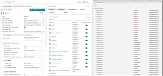
Alternatively, I tried to use Repeater1 (also triggered by the ePWM1 ADCSOCA event) to delay the trigger of the bust block until all HighPrio-SOCs are acquired. In this case the bust block is triggered by Repeater1.
But sadly a get an assert while ADC Bust initialisation ADC_setBurstModeConfig() --> ASSERT(((uint16_t)trigger & ~((uint16_t)0x1FU)) == 0U). Initialisation code is CCS Theia 1.4.1 generated. What's the problem here?
Further question is there a smarter way to get what i want. Using pure round robin acquisition doesn't work. I have to much total SOCs. On the real project I have per ADC core always 4 high prio SOCs and 7 to 9 round robin SOCs.
With best regards, Martin
Hi Martin,
Looks like there is only one ISR function in your code base on the snaphots provided, which is __interrupt void INT_myADC0_1_ISR() which is only mapped to ADCINT1 (INT_ADCA1). Clearing and acknowledging the other ISRs seems to be happening in that ISR routine. This is probably the reason why you are not seeing the expected results.
You would need to create 3 more ISR functions for each of the ISRs INT_ADCA2, INT_ADCA3 and INT_ADCA4, map/register these additional ISR to the interrupt controller using Interrupt_register() function and enable them using the Interrupt_enable() function. Lastly, remove the clearing and acknowledging of the other interrupts in INT_myADC0_1_ISR() and transfer these accordingly to the corresponding ISRs.
Regards,
Joseph
Hi Joseph,
thank you very much for your reply. In fact INT_myADC0_1_ISR() was mapped to ADCINT1 (INT_ADCA1), ADCINT2 (INT_ADCA2) and ADCINT3 (INT_ADCA3). But one ISR for all three IRQs was sloppy nevertheless, so I implemented your recommendations just to be sure.
Sadly the behavior is just the same. At that moment I enter INT_myADC0_1_ISR() (which should be entered after SOC1 EOC) for the first time after pressing RUN, all other SOCs: "SOC2 to SOC5" and "SOC7 to SOC9" are already acquired.
Just to recap, what I expect with my code: ePWM1 ADCSOCA event triggers the HighPrio-SOCs and the RR-Burst --> HighPrio-SOCs should come first --> SOC0 is acquired --> SOC1 is acquired --> SOC1 EOC IRQ is raised --> INT_myADC0_1_ISR() is called --> when I break in INT_myADC0_1_ISR(), I expect register ADCRESULT0 and ADCRESULT1 to have a value other than 0x000 and all other registers ADCRESULTx to have a value of 0x0000. Which they dont have.
For me, it just looks like that all of the SOCs triggered by ePWM1 ADCSOCA will be acquired first, and than afterwards all of the IRQs raised while acquirering SOCs will be handled, which doesnt seem right.
I added all of the relevant configuration,I hope that helps. Maybe I forgot to check a box.
Furthermore, is there any chance to halt the ADC core while pending on a breakpoint. Other controllers have something like: "Stop PWM/Timer while breaking", configurable with the help of a function, a asm-directive or via a register. Maybe Im getting fooled by the debugger. My theory is, the code is just fine, but the ADC core doesnt stop at the breakpoint and continues to acquire all other SOCs and at that moment the IDE is finally notified/updated all the results are written in the ADC result registers.
I hope you can help me in this matter.
With best regards,
Martin
Hi Martin,
Ok, let's inspect some ADC register contents to see what's going on. In the Register view, can you display AdcaRegs.ADCINTOVF (ADC overflow register) as below:
Also display some Peripheral Interrupt registers specifically PieCtrlRegs.PIEIER1 and PIEIER10 and expand to show the individual fields as below:
Setting a breakpoint inside the ADC ISR halts the conversions and prevents the update of the ADC results registers.
Regards,
Joseph
Hi Joseph,
"Setting a breakpoint inside the ADC ISR halts the conversions and prevents the update of the ADC results registers."
Than it seem like, SOCs are all acquired before the first ISR is called.
Here I got the screen shots you asked me about. Once again, the program was held the fist time after pressing "Run" in ADCA_INT1_ISR INT_myADC0_1_ISR() after (supposedly) the SOC1 EOC event.
Please notice, I continued steppig through the program from breakpoint to breakpoint but a "1" in any of AdcaRegs.ADCINTOVFs register never came up.
I hope you maybe see something, which I dont.
Best regards,
Martin
Hi Martin,
Thanks for providing the register snapshots. I'm able to get the information i needed based on the register contents. Interrupt 1-4 mapping is correct and interrupts seem to be firing based on the flags. I can also see that SOC0 is mapped to ADC CH1 while SOC1 to SOC5 is mapped to ADC CH0 and TRIGSEL for SOC0-5 is EPWM. SOC7-9 are triggered with SW (TRIGSEL=0) and channel is mapped to CH0, CH1 and CH2 respectively. Just wanted to confirm that this was the intent and you have the physical channels connected to signal sources.
Regards,
Joseph
Hi Joseph,
Im using the TI LauchPad kit with TMS320F28P650DK9 on it. The software Im using is based on the TI code example "adc_ex11_burst_mode_epwm" hence the name of my project.
PWM is configured like this:
PWM configuration remains the same like in "adc_ex11_burst_mode_epwm". ADC part was modified by me, just to test my intended high prio/rr setup as a prove of concept for our coming project.
To your question: No there aren't any physical signal sources connected to the channels. It's just the LauchPad as it is. All sampled adc channels are floating. Could this be the problem?
For my prove of concept, I just wanted to see if my high prio/rr setup works and if the controller behaves in a comprehensible matter. SOC channel mapping for me in this case is insignificant. I just wanted to see, that values are sampled and that the values are sampled and interrupts are raised in me intended order.
High Prio:"TRIGSEL for SOC0-5 is EPWM": My intention, TRIGSEL EPWM triggers SOC0-5, ADC samples SOC0 first, than SOC1, than SOC2, .... , than SOC5.
Round Robin: "TRIGSEL for SOC7-9 is SW (TRIGSEL=0)": My intention, BURSTTRIGSEL is also EPWM and the burst mode trigger overrides the SW TRIGSEL for SOC7-9.
I hope i could provide all the information that you need.
With best regards
Martin
Hi Martin,
Yes, that could very well be the issue. I suggest that you assign physical channels to the SOCs so you can observe converted values. You can try using the 1.2V VDD as a signal source and configure VREFHI (as either internal or external) but take note also of whether jumper M4 is connected (in which case, it is configured to external VREF, M4 removed would be internal VREF mode). Other signal level you can connect to would be GND. With the 1.2V and GND as signal sources that you can connect to SOC channels, you should be able to have more predictable conversion values as opposed to indeterminate values from floating channels.
Best regards,
Joseph
Hi Joseph,
I did what you asked me to do.
But sadly it had no effect. The device/software behaves just like before. No IRQ at EOC, the first ISR only called after all SOCs were aquired.
What I did:
- Connected (just hard wired, no additional resistors used) GND to ADC_CH0 and connected 1.2V VDD to ADC_CH4 and ADC_CH5
- Pulled M4 to make sure internal VREF is used
- Addionally reconfigured ASYSCTRL in the .syscfg file to use the internal VREF of 2.5V
- Reconfigured ADC SOC in the .syscfg file to following:
High Prio: SOC0 --> CH4 (VDD), SOC1 -->CH0 (GND), SOC2 -->CH4 (VDD), SOC3 --> CH0 (GND), SOC4 -->CH4 (VDD), SOC5 -->CH0 (GND)
LowPrio RR: SOC7 --> CHN5 (VDD), SOC8 -->CHN0 (GND), SOC9 -->CHN5 (VDD),
SOC10 --> CHN0 (GND), SOC11 -->CHN5 (VDD), SOC12 -->CHN0 (GND),
SOC13 -->CHN5 (VDD), SOC14 -->CHN0 (GND), SOC15 -->CHN5 (VDD)
What I got:
ADC results made sense. For SOC0 I got 0x0793h: => 1939 --> (1939 / 4096 ~ 1.2V / 2.5V)
Other SOC showed my configured VDD -> GND -> VDD -> ... pattern.
Once again I attached all register screenshots. I hope this further helps finding the issue.
(But at first glance, register values before and after reconfiguration seem pretty even)
With best regards,
Martin
Hi Martin,
Can you send me the ADC_init() function that you have generated? I wanted to see the order on how you have setup the high and low priority conversions and how burst mode was set up.
Thanks,
Joseph
Hi Joseph,
I attached you the generated board.c file with ADC_init() in it.
/* * Copyright (c) 2020 Texas Instruments Incorporated - http://www.ti.com * All rights reserved. * * Redistribution and use in source and binary forms, with or without * modification, are permitted provided that the following conditions * are met: * * * Redistributions of source code must retain the above copyright * notice, this list of conditions and the following disclaimer. * * * Redistributions in binary form must reproduce the above copyright * notice, this list of conditions and the following disclaimer in the * documentation and/or other materials provided with the distribution. * * * Neither the name of Texas Instruments Incorporated nor the names of * its contributors may be used to endorse or promote products derived * from this software without specific prior written permission. * * THIS SOFTWARE IS PROVIDED BY THE COPYRIGHT HOLDERS AND CONTRIBUTORS "AS IS" * AND ANY EXPRESS OR IMPLIED WARRANTIES, INCLUDING, BUT NOT LIMITED TO, * THE IMPLIED WARRANTIES OF MERCHANTABILITY AND FITNESS FOR A PARTICULAR * PURPOSE ARE DISCLAIMED. IN NO EVENT SHALL THE COPYRIGHT OWNER OR * CONTRIBUTORS BE LIABLE FOR ANY DIRECT, INDIRECT, INCIDENTAL, SPECIAL, * EXEMPLARY, OR CONSEQUENTIAL DAMAGES (INCLUDING, BUT NOT LIMITED TO, * PROCUREMENT OF SUBSTITUTE GOODS OR SERVICES; LOSS OF USE, DATA, OR PROFITS; * OR BUSINESS INTERRUPTION) HOWEVER CAUSED AND ON ANY THEORY OF LIABILITY, * WHETHER IN CONTRACT, STRICT LIABILITY, OR TORT (INCLUDING NEGLIGENCE OR * OTHERWISE) ARISING IN ANY WAY OUT OF THE USE OF THIS SOFTWARE, * EVEN IF ADVISED OF THE POSSIBILITY OF SUCH DAMAGE. * */ #include "board.h" //***************************************************************************** // // Board Configurations // Initializes the rest of the modules. // Call this function in your application if you wish to do all module // initialization. // If you wish to not use some of the initializations, instead of the // Board_init use the individual Module_inits // //***************************************************************************** void Board_init() { EALLOW; PinMux_init(); ASYSCTL_init(); ADC_init(); INTERRUPT_init(); EDIS; } //***************************************************************************** // // PINMUX Configurations // //***************************************************************************** void PinMux_init() { // // PinMux for modules assigned to CPU1 // // // ANALOG -> myANALOGPinMux0 Pinmux // // Analog PinMux for A0/DACA_OUT GPIO_setPinConfig(GPIO_227_GPIO227); // AIO -> Analog mode selected GPIO_setAnalogMode(227, GPIO_ANALOG_ENABLED); // Analog PinMux for A1 GPIO_setPinConfig(GPIO_228_GPIO228); // AIO -> Analog mode selected GPIO_setAnalogMode(228, GPIO_ANALOG_ENABLED); // Analog PinMux for A10, GPIO213 GPIO_setPinConfig(GPIO_213_GPIO213); // AGPIO -> Analog mode selected GPIO_setAnalogMode(213, GPIO_ANALOG_ENABLED); // Analog PinMux for A11, GPIO214 GPIO_setPinConfig(GPIO_214_GPIO214); // AGPIO -> Analog mode selected GPIO_setAnalogMode(214, GPIO_ANALOG_ENABLED); // Analog PinMux for A14/B14/C14 GPIO_setPinConfig(GPIO_225_GPIO225); // AIO -> Analog mode selected GPIO_setAnalogMode(225, GPIO_ANALOG_ENABLED); // Analog PinMux for A15/B15/C15 GPIO_setPinConfig(GPIO_226_GPIO226); // AIO -> Analog mode selected GPIO_setAnalogMode(226, GPIO_ANALOG_ENABLED); // Analog PinMux for A2 GPIO_setPinConfig(GPIO_229_GPIO229); // AIO -> Analog mode selected GPIO_setAnalogMode(229, GPIO_ANALOG_ENABLED); // Analog PinMux for A3 GPIO_setPinConfig(GPIO_230_GPIO230); // AIO -> Analog mode selected GPIO_setAnalogMode(230, GPIO_ANALOG_ENABLED); // Analog PinMux for A4 GPIO_setPinConfig(GPIO_231_GPIO231); // AIO -> Analog mode selected GPIO_setAnalogMode(231, GPIO_ANALOG_ENABLED); // Analog PinMux for A5 GPIO_setPinConfig(GPIO_232_GPIO232); // AIO -> Analog mode selected GPIO_setAnalogMode(232, GPIO_ANALOG_ENABLED); // Analog PinMux for A6, GPIO209 GPIO_setPinConfig(GPIO_209_GPIO209); // AGPIO -> Analog mode selected GPIO_setAnalogMode(209, GPIO_ANALOG_ENABLED); // Analog PinMux for A7, GPIO210 GPIO_setPinConfig(GPIO_210_GPIO210); // AGPIO -> Analog mode selected GPIO_setAnalogMode(210, GPIO_ANALOG_ENABLED); // Analog PinMux for A8, GPIO211 GPIO_setPinConfig(GPIO_211_GPIO211); // AGPIO -> Analog mode selected GPIO_setAnalogMode(211, GPIO_ANALOG_ENABLED); // Analog PinMux for A9, GPIO212 GPIO_setPinConfig(GPIO_212_GPIO212); // AGPIO -> Analog mode selected GPIO_setAnalogMode(212, GPIO_ANALOG_ENABLED); // Analog PinMux for B0/VDAC GPIO_setPinConfig(GPIO_233_GPIO233); // AIO -> Analog mode selected GPIO_setAnalogMode(233, GPIO_ANALOG_ENABLED); // Analog PinMux for B1/DACC_OUT GPIO_setPinConfig(GPIO_234_GPIO234); // AIO -> Analog mode selected GPIO_setAnalogMode(234, GPIO_ANALOG_ENABLED); // Analog PinMux for B10, GPIO219 GPIO_setPinConfig(GPIO_219_GPIO219); // AGPIO -> Analog mode selected GPIO_setAnalogMode(219, GPIO_ANALOG_ENABLED); // Analog PinMux for B11 GPIO_setPinConfig(GPIO_240_GPIO240); // AIO -> Analog mode selected GPIO_setAnalogMode(240, GPIO_ANALOG_ENABLED); // Analog PinMux for B13 GPIO_setPinConfig(GPIO_238_GPIO238); // AIO -> Analog mode selected GPIO_setAnalogMode(238, GPIO_ANALOG_ENABLED); // Analog PinMux for B2 GPIO_setPinConfig(GPIO_235_GPIO235); // AIO -> Analog mode selected GPIO_setAnalogMode(235, GPIO_ANALOG_ENABLED); // Analog PinMux for B3 GPIO_setPinConfig(GPIO_236_GPIO236); // AIO -> Analog mode selected GPIO_setAnalogMode(236, GPIO_ANALOG_ENABLED); // Analog PinMux for B4, GPIO215 GPIO_setPinConfig(GPIO_215_GPIO215); // AGPIO -> Analog mode selected GPIO_setAnalogMode(215, GPIO_ANALOG_ENABLED); // Analog PinMux for B5, GPIO216 GPIO_setPinConfig(GPIO_216_GPIO216); // AGPIO -> Analog mode selected GPIO_setAnalogMode(216, GPIO_ANALOG_ENABLED); // Analog PinMux for B6, GPIO207 GPIO_setPinConfig(GPIO_207_GPIO207); // AGPIO -> Analog mode selected GPIO_setAnalogMode(207, GPIO_ANALOG_ENABLED); // Analog PinMux for B7, GPIO208 GPIO_setPinConfig(GPIO_208_GPIO208); // AGPIO -> Analog mode selected GPIO_setAnalogMode(208, GPIO_ANALOG_ENABLED); // Analog PinMux for B8, GPIO217 GPIO_setPinConfig(GPIO_217_GPIO217); // AGPIO -> Analog mode selected GPIO_setAnalogMode(217, GPIO_ANALOG_ENABLED); // Analog PinMux for B9, GPIO218 GPIO_setPinConfig(GPIO_218_GPIO218); // AGPIO -> Analog mode selected GPIO_setAnalogMode(218, GPIO_ANALOG_ENABLED); // Analog PinMux for C0, GPIO199 GPIO_setPinConfig(GPIO_199_GPIO199); // AGPIO -> Analog mode selected GPIO_setAnalogMode(199, GPIO_ANALOG_ENABLED); // Analog PinMux for C10 GPIO_setPinConfig(GPIO_241_GPIO241); // AIO -> Analog mode selected GPIO_setAnalogMode(241, GPIO_ANALOG_ENABLED); // Analog PinMux for C11 GPIO_setPinConfig(GPIO_242_GPIO242); // AIO -> Analog mode selected GPIO_setAnalogMode(242, GPIO_ANALOG_ENABLED); // Analog PinMux for C13 GPIO_setPinConfig(GPIO_239_GPIO239); // AIO -> Analog mode selected GPIO_setAnalogMode(239, GPIO_ANALOG_ENABLED); // Analog PinMux for C2 GPIO_setPinConfig(GPIO_237_GPIO237); // AIO -> Analog mode selected GPIO_setAnalogMode(237, GPIO_ANALOG_ENABLED); // Analog PinMux for C3, GPIO206 GPIO_setPinConfig(GPIO_206_GPIO206); // AGPIO -> Analog mode selected GPIO_setAnalogMode(206, GPIO_ANALOG_ENABLED); // Analog PinMux for C4, GPIO205 GPIO_setPinConfig(GPIO_205_GPIO205); // AGPIO -> Analog mode selected GPIO_setAnalogMode(205, GPIO_ANALOG_ENABLED); // Analog PinMux for C5, GPIO204 GPIO_setPinConfig(GPIO_204_GPIO204); // AGPIO -> Analog mode selected GPIO_setAnalogMode(204, GPIO_ANALOG_ENABLED); // Analog PinMux for C6, GPIO203 GPIO_setPinConfig(GPIO_203_GPIO203); // AGPIO -> Analog mode selected GPIO_setAnalogMode(203, GPIO_ANALOG_ENABLED); // Analog PinMux for C1, GPIO200 GPIO_setPinConfig(GPIO_200_GPIO200); // AGPIO -> Analog mode selected GPIO_setAnalogMode(200, GPIO_ANALOG_ENABLED); // Analog PinMux for C7, GPIO198 GPIO_setPinConfig(GPIO_198_GPIO198); // AGPIO -> Analog mode selected GPIO_setAnalogMode(198, GPIO_ANALOG_ENABLED); // Analog PinMux for C8, GPIO202 GPIO_setPinConfig(GPIO_202_GPIO202); // AGPIO -> Analog mode selected GPIO_setAnalogMode(202, GPIO_ANALOG_ENABLED); // Analog PinMux for C9, GPIO201 GPIO_setPinConfig(GPIO_201_GPIO201); // AGPIO -> Analog mode selected GPIO_setAnalogMode(201, GPIO_ANALOG_ENABLED); } //***************************************************************************** // // ADC Configurations // //***************************************************************************** void ADC_init(){ myADC0_init(); } void myADC0_init(){ // // ADC Initialization: Write ADC configurations and power up the ADC // // Set the analog voltage reference selection and ADC module's offset trims. // This function sets the analog voltage reference to internal (with the reference voltage of 1.65V or 2.5V) or external for ADC // which is same as ASysCtl APIs. // ADC_setVREF(myADC0_BASE, ADC_REFERENCE_INTERNAL, ADC_REFERENCE_2_5V); // // Configures the analog-to-digital converter module prescaler. // ADC_setPrescaler(myADC0_BASE, ADC_CLK_DIV_4_0); // // Configures the analog-to-digital converter resolution and signal mode. // ADC_setMode(myADC0_BASE, ADC_RESOLUTION_12BIT, ADC_MODE_SINGLE_ENDED); // // Sets the timing of the end-of-conversion pulse // ADC_setInterruptPulseMode(myADC0_BASE, ADC_PULSE_END_OF_CONV); // // Powers up the analog-to-digital converter core. // ADC_enableConverter(myADC0_BASE); // // Delay for 1ms to allow ADC time to power up // DEVICE_DELAY_US(5000); // // Enable alternate timings for DMA trigger // ADC_enableAltDMATiming(myADC0_BASE); // // SOC Configuration: Setup ADC EPWM channel and trigger settings // // Enables SOC burst mode. // ADC_enableBurstMode(myADC0_BASE); // // Set SOC burst mode. // ADC_setBurstModeConfig(myADC0_BASE, ADC_TRIGGER_EPWM1_SOCA, 3); // // Sets the priority mode of the SOCs. // ADC_setSOCPriority(myADC0_BASE, ADC_PRI_THRU_SOC6_HIPRI); // // Start of Conversion 0 Configuration // // // Configures a start-of-conversion (SOC) in the ADC and its interrupt SOC trigger. // SOC number : 0 // Trigger : ADC_TRIGGER_EPWM1_SOCA // Channel : ADC_CH_ADCIN4 // Sample Window : 58 SYSCLK cycles // Interrupt Trigger: ADC_INT_SOC_TRIGGER_NONE // ADC_setupSOC(myADC0_BASE, ADC_SOC_NUMBER0, ADC_TRIGGER_EPWM1_SOCA, ADC_CH_ADCIN4, 58U); ADC_setInterruptSOCTrigger(myADC0_BASE, ADC_SOC_NUMBER0, ADC_INT_SOC_TRIGGER_NONE); // // Start of Conversion 1 Configuration // // // Configures a start-of-conversion (SOC) in the ADC and its interrupt SOC trigger. // SOC number : 1 // Trigger : ADC_TRIGGER_EPWM1_SOCA // Channel : ADC_CH_ADCIN0 // Sample Window : 45 SYSCLK cycles // Interrupt Trigger: ADC_INT_SOC_TRIGGER_NONE // ADC_setupSOC(myADC0_BASE, ADC_SOC_NUMBER1, ADC_TRIGGER_EPWM1_SOCA, ADC_CH_ADCIN0, 45U); ADC_setInterruptSOCTrigger(myADC0_BASE, ADC_SOC_NUMBER1, ADC_INT_SOC_TRIGGER_NONE); // // Start of Conversion 2 Configuration // // // Configures a start-of-conversion (SOC) in the ADC and its interrupt SOC trigger. // SOC number : 2 // Trigger : ADC_TRIGGER_EPWM1_SOCA // Channel : ADC_CH_ADCIN4 // Sample Window : 57 SYSCLK cycles // Interrupt Trigger: ADC_INT_SOC_TRIGGER_NONE // ADC_setupSOC(myADC0_BASE, ADC_SOC_NUMBER2, ADC_TRIGGER_EPWM1_SOCA, ADC_CH_ADCIN4, 57U); ADC_setInterruptSOCTrigger(myADC0_BASE, ADC_SOC_NUMBER2, ADC_INT_SOC_TRIGGER_NONE); // // Start of Conversion 3 Configuration // // // Configures a start-of-conversion (SOC) in the ADC and its interrupt SOC trigger. // SOC number : 3 // Trigger : ADC_TRIGGER_EPWM1_SOCA // Channel : ADC_CH_ADCIN0 // Sample Window : 15 SYSCLK cycles // Interrupt Trigger: ADC_INT_SOC_TRIGGER_NONE // ADC_setupSOC(myADC0_BASE, ADC_SOC_NUMBER3, ADC_TRIGGER_EPWM1_SOCA, ADC_CH_ADCIN0, 15U); ADC_setInterruptSOCTrigger(myADC0_BASE, ADC_SOC_NUMBER3, ADC_INT_SOC_TRIGGER_NONE); // // Start of Conversion 4 Configuration // // // Configures a start-of-conversion (SOC) in the ADC and its interrupt SOC trigger. // SOC number : 4 // Trigger : ADC_TRIGGER_EPWM1_SOCA // Channel : ADC_CH_ADCIN4 // Sample Window : 15 SYSCLK cycles // Interrupt Trigger: ADC_INT_SOC_TRIGGER_NONE // ADC_setupSOC(myADC0_BASE, ADC_SOC_NUMBER4, ADC_TRIGGER_EPWM1_SOCA, ADC_CH_ADCIN4, 15U); ADC_setInterruptSOCTrigger(myADC0_BASE, ADC_SOC_NUMBER4, ADC_INT_SOC_TRIGGER_NONE); // // Start of Conversion 5 Configuration // // // Configures a start-of-conversion (SOC) in the ADC and its interrupt SOC trigger. // SOC number : 5 // Trigger : ADC_TRIGGER_EPWM1_SOCA // Channel : ADC_CH_ADCIN0 // Sample Window : 15 SYSCLK cycles // Interrupt Trigger: ADC_INT_SOC_TRIGGER_NONE // ADC_setupSOC(myADC0_BASE, ADC_SOC_NUMBER5, ADC_TRIGGER_EPWM1_SOCA, ADC_CH_ADCIN0, 15U); ADC_setInterruptSOCTrigger(myADC0_BASE, ADC_SOC_NUMBER5, ADC_INT_SOC_TRIGGER_NONE); // // Start of Conversion 7 Configuration // // // Configures a start-of-conversion (SOC) in the ADC and its interrupt SOC trigger. // SOC number : 7 // Trigger : ADC_TRIGGER_SW_ONLY // Channel : ADC_CH_ADCIN5 // Sample Window : 15 SYSCLK cycles // Interrupt Trigger: ADC_INT_SOC_TRIGGER_NONE // ADC_setupSOC(myADC0_BASE, ADC_SOC_NUMBER7, ADC_TRIGGER_SW_ONLY, ADC_CH_ADCIN5, 15U); ADC_setInterruptSOCTrigger(myADC0_BASE, ADC_SOC_NUMBER7, ADC_INT_SOC_TRIGGER_NONE); // // Start of Conversion 8 Configuration // // // Configures a start-of-conversion (SOC) in the ADC and its interrupt SOC trigger. // SOC number : 8 // Trigger : ADC_TRIGGER_SW_ONLY // Channel : ADC_CH_ADCIN0 // Sample Window : 58 SYSCLK cycles // Interrupt Trigger: ADC_INT_SOC_TRIGGER_NONE // ADC_setupSOC(myADC0_BASE, ADC_SOC_NUMBER8, ADC_TRIGGER_SW_ONLY, ADC_CH_ADCIN0, 58U); ADC_setInterruptSOCTrigger(myADC0_BASE, ADC_SOC_NUMBER8, ADC_INT_SOC_TRIGGER_NONE); // // Start of Conversion 9 Configuration // // // Configures a start-of-conversion (SOC) in the ADC and its interrupt SOC trigger. // SOC number : 9 // Trigger : ADC_TRIGGER_SW_ONLY // Channel : ADC_CH_ADCIN5 // Sample Window : 45 SYSCLK cycles // Interrupt Trigger: ADC_INT_SOC_TRIGGER_NONE // ADC_setupSOC(myADC0_BASE, ADC_SOC_NUMBER9, ADC_TRIGGER_SW_ONLY, ADC_CH_ADCIN5, 45U); ADC_setInterruptSOCTrigger(myADC0_BASE, ADC_SOC_NUMBER9, ADC_INT_SOC_TRIGGER_NONE); // // Start of Conversion 10 Configuration // // // Configures a start-of-conversion (SOC) in the ADC and its interrupt SOC trigger. // SOC number : 10 // Trigger : ADC_TRIGGER_SW_ONLY // Channel : ADC_CH_ADCIN0 // Sample Window : 15 SYSCLK cycles // Interrupt Trigger: ADC_INT_SOC_TRIGGER_NONE // ADC_setupSOC(myADC0_BASE, ADC_SOC_NUMBER10, ADC_TRIGGER_SW_ONLY, ADC_CH_ADCIN0, 15U); ADC_setInterruptSOCTrigger(myADC0_BASE, ADC_SOC_NUMBER10, ADC_INT_SOC_TRIGGER_NONE); // // Start of Conversion 11 Configuration // // // Configures a start-of-conversion (SOC) in the ADC and its interrupt SOC trigger. // SOC number : 11 // Trigger : ADC_TRIGGER_SW_ONLY // Channel : ADC_CH_ADCIN5 // Sample Window : 58 SYSCLK cycles // Interrupt Trigger: ADC_INT_SOC_TRIGGER_NONE // ADC_setupSOC(myADC0_BASE, ADC_SOC_NUMBER11, ADC_TRIGGER_SW_ONLY, ADC_CH_ADCIN5, 58U); ADC_setInterruptSOCTrigger(myADC0_BASE, ADC_SOC_NUMBER11, ADC_INT_SOC_TRIGGER_NONE); // // Start of Conversion 12 Configuration // // // Configures a start-of-conversion (SOC) in the ADC and its interrupt SOC trigger. // SOC number : 12 // Trigger : ADC_TRIGGER_SW_ONLY // Channel : ADC_CH_ADCIN0 // Sample Window : 58 SYSCLK cycles // Interrupt Trigger: ADC_INT_SOC_TRIGGER_NONE // ADC_setupSOC(myADC0_BASE, ADC_SOC_NUMBER12, ADC_TRIGGER_SW_ONLY, ADC_CH_ADCIN0, 58U); ADC_setInterruptSOCTrigger(myADC0_BASE, ADC_SOC_NUMBER12, ADC_INT_SOC_TRIGGER_NONE); // // Start of Conversion 13 Configuration // // // Configures a start-of-conversion (SOC) in the ADC and its interrupt SOC trigger. // SOC number : 13 // Trigger : ADC_TRIGGER_SW_ONLY // Channel : ADC_CH_ADCIN5 // Sample Window : 48 SYSCLK cycles // Interrupt Trigger: ADC_INT_SOC_TRIGGER_NONE // ADC_setupSOC(myADC0_BASE, ADC_SOC_NUMBER13, ADC_TRIGGER_SW_ONLY, ADC_CH_ADCIN5, 48U); ADC_setInterruptSOCTrigger(myADC0_BASE, ADC_SOC_NUMBER13, ADC_INT_SOC_TRIGGER_NONE); // // Start of Conversion 14 Configuration // // // Configures a start-of-conversion (SOC) in the ADC and its interrupt SOC trigger. // SOC number : 14 // Trigger : ADC_TRIGGER_SW_ONLY // Channel : ADC_CH_ADCIN0 // Sample Window : 46 SYSCLK cycles // Interrupt Trigger: ADC_INT_SOC_TRIGGER_NONE // ADC_setupSOC(myADC0_BASE, ADC_SOC_NUMBER14, ADC_TRIGGER_SW_ONLY, ADC_CH_ADCIN0, 46U); ADC_setInterruptSOCTrigger(myADC0_BASE, ADC_SOC_NUMBER14, ADC_INT_SOC_TRIGGER_NONE); // // Start of Conversion 15 Configuration // // // Configures a start-of-conversion (SOC) in the ADC and its interrupt SOC trigger. // SOC number : 15 // Trigger : ADC_TRIGGER_SW_ONLY // Channel : ADC_CH_ADCIN5 // Sample Window : 46 SYSCLK cycles // Interrupt Trigger: ADC_INT_SOC_TRIGGER_NONE // ADC_setupSOC(myADC0_BASE, ADC_SOC_NUMBER15, ADC_TRIGGER_SW_ONLY, ADC_CH_ADCIN5, 46U); ADC_setInterruptSOCTrigger(myADC0_BASE, ADC_SOC_NUMBER15, ADC_INT_SOC_TRIGGER_NONE); // // ADC Interrupt 1 Configuration // Source : ADC_INT_TRIGGER_EOC1 // Interrupt Source: enabled // Continuous Mode : disabled // // ADC_setInterruptSource(myADC0_BASE, ADC_INT_NUMBER1, ADC_INT_TRIGGER_EOC1); ADC_clearInterruptStatus(myADC0_BASE, ADC_INT_NUMBER1); ADC_disableContinuousMode(myADC0_BASE, ADC_INT_NUMBER1); ADC_enableInterrupt(myADC0_BASE, ADC_INT_NUMBER1); // // ADC Interrupt 2 Configuration // Source : ADC_INT_TRIGGER_EOC3 // Interrupt Source: enabled // Continuous Mode : disabled // // ADC_setInterruptSource(myADC0_BASE, ADC_INT_NUMBER2, ADC_INT_TRIGGER_EOC3); ADC_clearInterruptStatus(myADC0_BASE, ADC_INT_NUMBER2); ADC_disableContinuousMode(myADC0_BASE, ADC_INT_NUMBER2); ADC_enableInterrupt(myADC0_BASE, ADC_INT_NUMBER2); // // ADC Interrupt 3 Configuration // Source : ADC_INT_TRIGGER_EOC5 // Interrupt Source: enabled // Continuous Mode : disabled // // ADC_setInterruptSource(myADC0_BASE, ADC_INT_NUMBER3, ADC_INT_TRIGGER_EOC5); ADC_clearInterruptStatus(myADC0_BASE, ADC_INT_NUMBER3); ADC_disableContinuousMode(myADC0_BASE, ADC_INT_NUMBER3); ADC_enableInterrupt(myADC0_BASE, ADC_INT_NUMBER3); // // ADC Interrupt 4 Configuration // Source : ADC_INT_TRIGGER_EOC9 // Interrupt Source: enabled // Continuous Mode : disabled // // ADC_setInterruptSource(myADC0_BASE, ADC_INT_NUMBER4, ADC_INT_TRIGGER_EOC9); ADC_clearInterruptStatus(myADC0_BASE, ADC_INT_NUMBER4); ADC_disableContinuousMode(myADC0_BASE, ADC_INT_NUMBER4); ADC_enableInterrupt(myADC0_BASE, ADC_INT_NUMBER4); } //***************************************************************************** // // ASYSCTL Configurations // //***************************************************************************** void ASYSCTL_init(){ // // asysctl initialization // // Disables the temperature sensor output to the ADC. // ASysCtl_disableTemperatureSensor(); // // Set the analog voltage reference selection to internal. // ASysCtl_setAnalogReferenceInternal( ASYSCTL_VREFHIA | ASYSCTL_VREFHIB | ASYSCTL_VREFHIC ); // // Set the internal analog voltage reference selection to 2.5V. // ASysCtl_setAnalogReference2P5( ASYSCTL_VREFHIA | ASYSCTL_VREFHIB | ASYSCTL_VREFHIC ); } //***************************************************************************** // // INTERRUPT Configurations // //***************************************************************************** void INTERRUPT_init(){ // Interrupt Settings for INT_myADC0_1 Interrupt_register(INT_myADC0_1, &INT_myADC0_1_ISR); Interrupt_enable(INT_myADC0_1); // Interrupt Settings for INT_myADC0_2 Interrupt_register(INT_myADC0_2, &INT_myADC0_2_ISR); Interrupt_enable(INT_myADC0_2); // Interrupt Settings for INT_myADC0_3 Interrupt_register(INT_myADC0_3, &INT_myADC0_3_ISR); Interrupt_enable(INT_myADC0_3); // Interrupt Settings for INT_myADC0_4 Interrupt_register(INT_myADC0_4, &INT_myADC0_4_ISR); Interrupt_enable(INT_myADC0_4); }
With best regards,
Martin
Hello Martin,
There were some missing dependencies like the ISR and since the code is automatically generated through SysConfig, I can't really override the changes you made so I started with adc_ex11_burst_mode_epwm example and made the following changes through SysConfig except for step4 which is manually adding the ISR function in the c file. Below are the steps:
1.) Register PIE Interrupt Handlers
2.) ADC INT Configurations
3.) SOC Configurations
4.) Add ISR for the high priority conversions at the bottom of adc_ex11_burst_mode_epwm.c file:
__interrupt void INT_myADC0_4_ISR(void)
{
// Add codes here to read out high priority SOC result values
// adcAResult0 = ADC_readResult(ADCARESULT_BASE, ADC_SOC_NUMBER0);
// adcAResult1 = ADC_readResult(ADCARESULT_BASE, ADC_SOC_NUMBER1);
ADC_clearInterruptStatus(ADCA_BASE, ADC_INT_NUMBER4);
Interrupt_clearACKGroup(INTERRUPT_ACK_GROUP10);
}
The ISR in the original example handles the round robin priority for INT1 to INT3. The additional ISR handles the high priority conversions and is using INT4. You can basically set up breakpoints in the high priority conversions as well as in the round robin ISR inside the existing adcABurstISR in each burst and step through them. I think this is what you are trying to accomplish. I can step through the breakpoints in the high priority conversions as well as the individual burst inside adcABurstISR with no issues. Let me know if this works for you.
Best Regards,
Joseph
Hi Joseph,
I set up a new project based one the adc_ex11_burst_mode_epwm example and just extended it accordingly to your recommendations steps 1 to 4.
I added nothing more. For HighPrio I used SOC0 to SOC3, all SOC are set to CH4, all are triggered by ePWM1, ADCSOCA and all sample the voltage VDD = 1.2V (at tsample = 15 cycles) and with the VREF (intern) = 1.65 V as the reference.
SOC7 to SOC 15 use the old VDD, GND, VDD pattern.
Sadly, once again I see low prio SOC7 to SOC9 acquired, while breaking at ADC_INT4 ISR. This should not be happening, because ADC_INT4 ISR should be called right after SOC3 EOC, and ADC0 core should be on hold while breaking at ADC_INT4 ISR.
Once again I have the strong feeling that my high prio ISR (in this case ADC_INT4 ISR) was called after SOC9 EOC.
This theory is further reinforced by the fact that the INTx1 Flag is raised in the PIEIFR1 register.
Why am I so keen on getting my ISR called with no further delay.
For our project ePWM1 is running at 100 kHz, in center alligned, up-down-mode. Time from Z to Z = 10 µs, time from P to Z = 5 µs. We want to start the sampling of important (high prio) values the last time before calling our controller right at P: So we have 5 µs time to "sample and convert soc0 to soc3" and "processing our ac controller" and "shadow our new dutycycle" till Z arrives.
One of our SOC takes approximately 500 ns:
--> 4 (only high prio) x 500 ns = 2 µs --> 5 µs - 2 µs = 3 µs (plenty of time for processing our ac controller)
--> 7 (high prio + rr) x 500 ns = 3,5 µs --> 5 µs - 3,5 µs = 1,5 µs (not enough time for processing our ac controller)
I'd like to ask you once more, if this kind of behavior is typical for the C2000 ADC. Maybe I need to start to work on workarounds.
Please can you provide this or further information?
With best regards,
Martin
Hi Martin,
Ok, let me research more on this one. The high priority and the round robin triggers are both sourced from same EPWMSOC so not sure how this affects priority and the RR. Also I assume P to Z is the SOCA counter trigger?
Regards,
Joseph
Hi Joseph,
the P-Event off the up-down counting ePWM is the SOCA trigger, which will start high prio SOCs and the RR burst. You are correct.
We also need to be done with all (sampling + calculations) before reaching Z (the Update-Event) off the ePWM.
As a possible workaround, we will have some synched up ePWMs anyway. I could use the ePWM1 SOCA to trigger all the high prio SOC as it is and could synch up an additional (sacrificial) ePWM with a fixed dutycucle, just to generate an additional SOCA trigger, one cycle after the ePWM1 P-Event (ePWM1 SOCA) to trigger all the RR bursts. Sounds a little bit contrived to me, but if it works it works.
Best regards,
Martin
Hi Martin,
Ok, here's what I found out with the example we were running with high priority and RR burst if both high priority and RR burst conversions are triggered by EPWMSOCA:
First trigger : SOC 0–6 followed by SOC 7,8,9
Second trigger : SOC 0-6 followed by SOC 10, 11, 12
Third trigger: SOC 0-6 followed by SOC 13,14,15
Regarding to your application, the last diagram you shared makes it clear to me now what you are trying to accomplish. You are assigning high priority for the 3ph grid ac voltage conversions and load current sampling and the RR is for the DC link sampling, fan, temperature + some other monitor signals. Maybe what you can do is assign another ISR for the RR and do the calculations exclusively for each ISR. Would calculation/processing time be smaller for only the RR signals? If such is the case, maybe you can organize the conversion/ISRs as below diagram for 1 ADC:
Another option is to set P earlier such that the EPWM SOC trigger occurs earlier, maybe at a count of 1uS after Z initializes to 0. This will give plenty of time (9uS) for sampling + calculation for priority SOCs and RR for 100Khz PWM period.
Lastly, we can revisit how the 500ns conversion was derived. This has to do with the conversion mode, ADC speed and what is planned for your input network. If signal conditioning and buffering are properly taken care of, you should be able to attain the fastest sampling time and reduce the SH+conversion time further.
Best regards,
joseph
Hi Joseph,
sorry for the late late reply.
I think I found a solution for my problem. And thanks for your input.
High Prio SOCs come 2 times per period, triggered bei e.g. ePWM7 ADCSOCA (ETINTMIX = ZERO || PERIOD)
Low Prio Bursts also come 2 times per period, triggered bei e.g. ePWM8 ADCSOCA (ETINTMIX = CMPA_INCREMENT || CMPA_DECREMENT)
Period is 10 µs, so the time windows for 4 samples are 2.5 µs and I can rearrange my SOC blocks if I have to, I kinda like it. So case closed, I think.
--------------------------------------------------------------------------------------------------------------------------------------------------------------------------------------------
There is just one last thing.
Also I have found out that ADC cores really dont seem to stop if hitting debugger breakpoints.
But at least the interrupt does fire at the exact moment I need it to trigger. So, the whole time I kinda chased a problem which wasn`t really there.
I think I have the proof right here:
I build a new project.
ADCA is fed by SYSCLK at 200 MHz and runs at 50 MHz (Divider at 4)
ADCA SOC0 to SCO3 are all at15 SYSCLK cycles for sampling
ADCA SOC7 to SCO9 are all at15 SYSCLK cycles for sampling
ePWM1 also fed by SYSCLK and runs at 200 MHz (Time Base Clock Divider and High Speed Clock Divider both at 1), so ePWM1 TBCTR also doubles as a SYSCYL counter
ePWM1 period is at 1999, up counting, counter stops on next increment after emulator stop
ePWM1 CMPA is at 1000
ePWM1 ADCSOCA is triggered by CMPA_INCREMENTING, which triggers ADCA SOCs 0 to 3 and ADCA Burst SOCs 7 to 9
ePWM1 CMPA_INCREMENTING also triggeres the PWM interrupt "INT_myEPWM1_ISR"
ADCA SOC3 ECO triggeres the ADC interrupt "INT_myADC0_1_ISR"
ADCA SOC9 ECO triggeres the ADC interrupt "INT_myADC0_2_ISR"
Like always, SOC7 to SOC9 have already been sampled and converted, when the IDE showed me the "INT_myADC0_1_ISR". Because the ADCA core didn`t stop, right at the moment while hitting a breakpoint. The core continued so resolve the burst trigger, before finally stopping only after all burst SOCs where sampled and converted.
I set a breakpoint in "INT_myEPWM1_ISR". The value of ePWM1 TBCTR (at breakpoint, in ISR after event CMPA_INCREMENTING) is 0x3FBh (1019dec)
(1019dec, sadly not 100% even to the 1000 CMPA value, but the value is reasonable, because some SYSCLK cycles passed after the CMPA_INCREMENTING event and before entering the ISR)
I set a breakpoint in "INT_myADC0_1_ISR".The value of ePWM1 TBCTR (at breakpoint, in ISR after event ADCA SOC3 ECO) is 0x472h (1138dec)
(1138dec- 1019dec equals to 119dec. At first glance this could be equal to 4 times 30 SYSCLK cycles for sampling and converting SOC0 to SOC3)
I set a breakpoint in "INT_myADC0_2_ISR". The value of ePWM1 TBCTR (at breakpoint, in ISR after event ADCA SOC9 ECO) is 0x546h (1350dec)
(1350dec- 1138dec equals to 212dec. At first glance this seems of, but INT_myADC0_1_ISR takes from 0x472h to 0x530h, so 3 times 30 SYSCLK cycles for sampling and converting SOC7 to SOC9 have already past before entering this ISR)
For me, looking at the ePWM1 TBCTR values (equal to SYSCLK cycles) confirms, that the ADCA core really doesn´t stop while breaking. Especially looking at the delta between 0x3FBh (1019dec) "INT_myEPWM1_ISR" (SOC trigger) and 0x472h (1138dec) "INT_myADC0_1_ISR" (final high prio SOC EOC trigger).
There is just one thing that´s a little bit funky.
I told you that 1138dec- 1019dec equals to 119dec which is equal to 4 times 30 SYSCLK cycles for sampling and converting SOC0 to SOC3. Which sadly doesn´t add up!
Tsample for SOC0 to SOC4 are all configured at 15 SYSCLK cycles. Also ADCA clock divider is at 4, which means Tconvert is at 41 SYSCLK cycles. With channel switching (2 SYSCLK cycles) and writing to register (2 SYSCLK cycles) this should all add up to 60 SYSCLK cycles per SOC. I expected the delta to be 240dec and not 119dec. Which means the SOCs in my project are aquired to fast. I searched and searched, but couldn´t find anything I configured incorrect.
Do you have any idea what I did wrong/whats going on?
With best regards.
Martin
Hi Martin,
Can you check on the value of PERCLKDIVSEL.EPWMCLKDIV in the register view? Just making sure SYSCLK is not pre scaled before going in to EPWM. Also, check on the count mode for EPWM time base. Is it up mode only or is it up/down? In up mode count, period is time base period count (TBPRD). In up/down mode period would be 2*TBPRD.
Regards,
Joseph
Hi Joseph,
I think they are looking fine.
I`m in pure up-counting mode.
(Just checking: For example, for any ePWM, base configs are 200 MHz go in, Time Base Clock Divider at 1, High Speed Clock Divider at 1
ePWM in up-mode: TBPRD at 1999 equals PWM at 100 kHz,
ePWM in up-down-mode: TBPRD at 999 also equals PWM at 100 kHz, right?)
Regards Martin
Hi Martin,
Clock prescalers are confusing A '0' is div by 1 and a '1' is div by 2. We generally add a 1 to get the actual divider for clock prescaler. It looks like EPWM is clocked at 100MHz before the time base divider and the high speed divider.
You can add this code in your main prior to setting up EPWM:
SysCtl_setEPWMClockDivider(SYSCTL_EPWMCLK_DIV_1);
Give this a shot and let me know. If this works we'll have to check on the clock tree tool to see why this is not obvious.
Regards,
Joseph
Hi Joseph,
thanks for the advice. It worked!
"INT_myEPWM1_ISR" comes at ePWM1 TBCTR 1036dec and "INT_myADC0_1_ISR" comes at ePWM1 TBCTR 1272dec. Round about a delta of 240dec.
It is the clock tree tool.
I commented "SysCtl_setEPWMClockDivider(SYSCTL_EPWMCLK_DIV_1);" and its backt to 100 MHz. Clock tree tool still stands at div 1 (should equal a 0 in reg).
Regards Martin
Hi Martin,
Glad to know this worked for you. Let me check with clock tree tool folks to see if there is anything they can recommend or need to fix.
Regards,
Joseph
Hi Joseph,
I remember, as I created a new project, I set EPWMCLKDIV manually from /2 to /1.
Right now I created a complete new empty project again.
EPWMCLKDIV was at /2 per default. I manually set EPWMCLKDIV from /2 to /1 again, cleaned, rebuild, downloaded and debugged.
No effect (see screen shot)
Maybe this could be a Theia thing, hope this helps. ;-)
For Info I´m on Theia 1.5.0
With best regards,
Martin
Hi Martin,
Yes, this is useful information for clock tree tool. I'll share this feedback to the team.
Regards,
joseph
Hi Martin,
Can you check if you can get to these screens and settings in your clock tree tool?
This should set the clock to EPWM equal to SYSCLK. Let me know if your code gets updated with the EPWM clock divider with this change and will feed it back to the clock tree tool folks.
Regards,
Joseph
Hi Joseph,
this is what I set up:
I selected SYSCLKDIVSEL and EPWMCLKDIV individually each and set them to /1.
Saved all, cleaned, rebuilt, downloaded and debugged.
Bonus, where the clock comes from:
But it had no effect.
-------------------------------------------------------------------------------------------------------------------------------------------
Also I tried something else (modified SYSCLKDIVSEL, LINACLKDIV andLINBCLKDIV,
saved all, cleaned, rebuilt, downloaded and debugged.), with this result:
It looks like, (for me at last) configurations in the tree config tool have no effect on code gen.
Regards Martin
Hi Martin,
Thank you for checking this out. I'll share this with our clocktree tool expert to get more insight on what could be happening.
Regards,
Joseph
Hi Martin,
As an additional step, you need to enable Device Support so that the change in clock tree will get populated in device.c file:
Ignore the other clock settings above...snippet just shows that EPWM clock divider gets changed here when Device Support is added. Check it out and let me know if this works for you.
Regards,
Joseph
Hi Joseph,
it worked! ;-) Thank you for helping me out.
------------------------------------------------------------------------------------------------------------------------------------------------------
One addition. With just adding Device Support I got redefinition linker errors. #10056
I tried https://e2e.ti.com/support/processors-group/processors/f/processors-forum/1309451/ccstudio-sysconfig-with-adding-device-support but without success.
If someone stumbles over this thread with the same problem in mind.
You need to exclude the whole device folder and let "Use Standard Code Start Branche" tagged in.
Than it compiles without issues.
With best regards,
Martin
Hi Joseph,
sorry for the late late reply.
I think I found a solution for my problem. And thanks for your input.
High Prio SOCs come 2 times per period, triggered bei e.g. ePWM7 ADCSOCA (ETINTMIX = ZERO || PERIOD)
Low Prio Bursts also come 2 times per period, triggered bei e.g. ePWM8 ADCSOCA (ETINTMIX = CMPA_INCREMENT || CMPA_DECREMENT)
Period is 10 µs, so the time windows for 4 samples are 2.5 µs and I can rearrange my SOC blocks if I have to, I kinda like it. So case closed, I think.
--------------------------------------------------------------------------------------------------------------------------------------------------------------------------------------------
There is just one last thing.
Also I have found out that ADC cores really dont seem to stop if hitting debugger breakpoints.
But at least the interrupt does fire at the exact moment I need it to trigger. So, the whole time I kinda chased a problem which wasn`t really there.
I think I have the proof right here:
I build a new project.
ADCA is fed by SYSCLK at 200 MHz and runs at 50 MHz (Divider at 4)
ADCA SOC0 to SCO3 are all at15 SYSCLK cycles for sampling
ADCA SOC7 to SCO9 are all at15 SYSCLK cycles for sampling
ePWM1 also fed by SYSCLK and runs at 200 MHz (Time Base Clock Divider and High Speed Clock Divider both at 1), so ePWM1 TBCTR also doubles as a SYSCYL counter
ePWM1 period is at 1999, up counting, counter stops on next increment after emulator stop
ePWM1 CMPA is at 1000
ePWM1 ADCSOCA is triggered by CMPA_INCREMENTING, which triggers ADCA SOCs 0 to 3 and ADCA Burst SOCs 7 to 9
ePWM1 CMPA_INCREMENTING also triggeres the PWM interrupt "INT_myEPWM1_ISR"
ADCA SOC3 ECO triggeres the ADC interrupt "INT_myADC0_1_ISR"
ADCA SOC9 ECO triggeres the ADC interrupt "INT_myADC0_2_ISR"
Like always, SOC7 to SOC9 have already been sampled and converted, when the IDE showed me the "INT_myADC0_1_ISR". Because the ADCA core didn`t stop, right at the moment while hitting a breakpoint. The core continued so resolve the burst trigger, before finally stopping only after all burst SOCs where sampled and converted.
I set a breakpoint in "INT_myEPWM1_ISR". The value of ePWM1 TBCTR (at breakpoint, in ISR after event CMPA_INCREMENTING) is 0x3FBh (1019dec)
(1019dec, sadly not 100% even to the 1000 CMPA value, but the value is reasonable, because some SYSCLK cycles passed after the CMPA_INCREMENTING event and before entering the ISR)
I set a breakpoint in "INT_myADC0_1_ISR".The value of ePWM1 TBCTR (at breakpoint, in ISR after event ADCA SOC3 ECO) is 0x472h (1138dec)
(1138dec- 1019dec equals to 119dec. At first glance this could be equal to 4 times 30 SYSCLK cycles for sampling and converting SOC0 to SOC3)
I set a breakpoint in "INT_myADC0_2_ISR". The value of ePWM1 TBCTR (at breakpoint, in ISR after event ADCA SOC9 ECO) is 0x546h (1350dec)
(1350dec- 1138dec equals to 212dec. At first glance this seems of, but INT_myADC0_1_ISR takes from 0x472h to 0x530h, so 3 times 30 SYSCLK cycles for sampling and converting SOC7 to SOC9 have already past before entering this ISR)
For me, looking at the ePWM1 TBCTR values (equal to SYSCLK cycles) confirms, that the ADCA core really doesn´t stop while breaking. Especially looking at the delta between 0x3FBh (1019dec) "INT_myEPWM1_ISR" (SOC trigger) and 0x472h (1138dec) "INT_myADC0_1_ISR" (final high prio SOC EOC trigger).
There is just one thing that´s a little bit funky.
I told you that 1138dec- 1019dec equals to 119dec which is equal to 4 times 30 SYSCLK cycles for sampling and converting SOC0 to SOC3. Which sadly doesn´t add up!
Tsample for SOC0 to SOC4 are all configured at 15 SYSCLK cycles. Also ADCA clock divider is at 4, which means Tconvert is at 41 SYSCLK cycles. With channel switching (2 SYSCLK cycles) and writing to register (2 SYSCLK cycles) this should all add up to 60 SYSCLK cycles per SOC. I expected the delta to be 240dec and not 119dec. Which means the SOCs in my project are aquired to fast. I searched and searched, but couldn´t find anything I configured incorrect.
Do you have any idea what I did wrong/whats going on?
With best regards.
Martin
Hi Martin,
At which point in the ISR did you set the breakpoint? Also can you check the value of TBCTL.FREE_SOFT field? Value of this field should be 0 so that any breakpoint would stop the time base counter. Another alternative to setting up the breakpoint in CCS is to write an ESTOP0; macro at the line you wish to put a breakpoint.
My guess is the counter is probably not reflecting the current value in the register. Seems like you want to profile the exact conversion times for the SOC combinations for your control loop. You can also do this with GPIO toggles and observe the toggle duration from a scope. GPIO function GPIO_writePin() will set the output of a GPIO provided that the GPIO is configured as an output. This function takes very few clock cycles to execute so it is one reliable way to profile time duration between different points in your code.
Regards,
Joseph
Hi Joseph,
is set the breakpoint at the first best line to set a breakpoint at (first line after function name, see screen shots above).
TBCTL.FREE_SOFT is also set to 0. But exact cycle count wasn't the problem. It was more of a problem, that 4 SOC seem to take 119 cycles instead of 240 cycles minimum.
--------------------------------------------------
But one question: Like I wrote "SW breaks at INT_myEPWM1_ISR at ePWM1 TBCTR 1036dec", interrupt is triggered at ePWM1 TBCTR 1000dec. Do 36dec cpu cycles from IRQ trigger to breaking at the ISR sound reasonable?
--------------------------------------------------
But I will gladly try ESTOP0; in the future and profiling via GPIOs also sounds like e really idea.
Instead of triggering the interrupt at SOC EOC, I plan indeed to trigger the interrupt at SOC S+H with an offset.
So proper profiling will definitely become a must have. SO thanks again for the advice.
Best regards,
Martin
Hi Martin,
There are several cpu cycles involved in entering ISR, servicing and acknowledging but 36 cycles may be too much. I'll have to check on other docs how much this actually entails.
in the meantime, it would be good to profile the steps with GPIO toggle. There is another option, which i am not familiar with but can have someone guide you with how to use this. This involves using ERAD and its purpose if for SW profiling. One drawback though is it's not yet supported in Theia but works on the older version on CCS. This may be another option to look at if the GPIO profiling would prove not to be reliable.
Regards,
Joseph