This thread has been locked.
If you have a related question, please click the "Ask a related question" button in the top right corner. The newly created question will be automatically linked to this question.
Tool/software:
We are doing the pre-production, the total 225 products have the below problem.
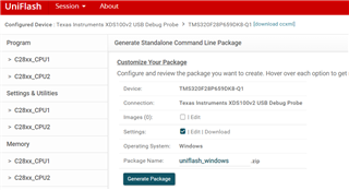
We use the uniflash to add the OTP.out, then generate the dslite-C28xx_CPU1.bat.
When flash the OTP.out file, call the generated the dslite-C28xx_CPU1.bat.
The first time, 100% happens below error: C28xx_CPU1: File Loader: Verification failed: Values at address 0x078000@Program do not match Please verify target memory and memory map.
Below is the completed log.
###Start 20240929 15:04:43 ReadyCheck_NAN### ###Start 20240929 15:04:43 Barcode_10### ###Start 20240929 15:04:44 AirCylinder_ON### ###Start 20240929 15:04:46 PowerON_### ###Start 20240929 15:04:47 DaleyTime_5### ###Start 20240929 15:04:52 UBoot_OPT_1### 20240929 15:04:52 "C:\FCT\Data\BurningFile\850-000407_3.0\DSP\OPT\dslite-C28xx_CPU1.bat" 20240929 15:05:14 Executing default command: > dslite --mode flash -c user_files/configs/f28p659dk8-q1.ccxml -l user_files/settings/generated.ufsettings -s VerifyAfterProgramLoad="No verification" -e -f -v "user_files/images/dcsm_security_tool_NT3(OTP).out" DSLite version 12.7.0.3382 Configuring Debugger (may take a few minutes on first launch)... Initializing Register Database... Initializing: IcePick_C_0 Executing Startup Scripts: IcePick_C_0 Initializing: C28xx_CPU1 Executing Startup Scripts: C28xx_CPU1 Initializing: CPU1_CLA1 Executing Startup Scripts: CPU1_CLA1 Initializing: C28xx_CPU2 Executing Startup Scripts: C28xx_CPU2 Initializing: JLM Executing Startup Scripts: JLM Connecting... C28xx_CPU1: GEL Output: Memory Map Initialization Complete C28xx_CPU1: GEL Output: ... DCSM Initialization Start ... C28xx_CPU1: GEL Output: ... DCSM Initialization Done ... C28xx_CPU1: GEL Output: CPU2 is out of reset and configured to wait boot. (If you connected previously, may have to resume CPU2 to reach wait boot loop.) info: C28xx_CPU1: If erase/program (E/P) operation is being done on one core, the other core should not execute from shared-RAM (SR) as they are used for the E/P code. User code execution from SR could commence after the selected CPU1/CPU2 flash banks executable are programmed. info: C28xx_CPU1: Only CPU1 on-chip Flash Plugin can configure clock for CPU1, and CPU2 Flash operations. Plugin automatically configures PLL when CPU1 Flash operations are invoked. However, if users want to do only CPU2 Flash operations without doing a prior CPU1 operation in the current session, they should click on 'Configure Clock' button in CPU1's on-chip Flash Plugin before invoking CPU2 Flash operations. When this button is used, Flash Plugin will configure the clock for CPU1/CPU2 at 200MHz using INTOSC as the clock source. Plugin will leave PLL config like this and user application should configure the PLL as required by application. info: C28xx_CPU1: Before doing any flash operations using the flash plugin, (a) Please select which flash banks should be mapped to which CPU (CPU1 vs CPU2) - This selection should be done in CPU1 flash plugin GUI. (b) Please select the flash banks that the user would like the flash plugin to erase (in the CPU1 flash plugin GUI and the CPU2 flash plugin GUI) C28xx_CPU1: GEL Output: ... DCSM Initialization Start ... C28xx_CPU1: GEL Output: ... DCSM Initialization Done ... C28xx_CPU1: GEL Output: CPU2 is out of reset and configured to wait boot. (If you connected previously, may have to resume CPU2 to reach wait boot loop.) Loading Program: user_files/images/dcsm_security_tool_NT3(OTP).out Preparing ... .data: 0 of 128 at 0x78000 C28xx_CPU1: GEL Output: ... DCSM Initialization Start ... C28xx_CPU1: GEL Output: ... DCSM Initialization Done ... C28xx_CPU1: GEL Output: CPU2 is out of reset and configured to wait boot. (If you connected previously, may have to resume CPU2 to reach wait boot loop.) info: C28xx_CPU1: GSxMSEL register configured correctly info: C28xx_CPU1: BankMuxSel register configured correctly Erasing Flash Erasing Bank 0 Erasing Bank 1: 20% Erasing Bank 2: 40% Erasing Bank 3: 60% Erasing Bank 4: 80% .text: 0 of 4 at 0x80000: 1% .data: 0 of 936 at 0x80008: 1% .text: 0 of 470 at 0x801e0: 15% .text: 0 of 5150 at 0x802d0: 22% .data: 0 of 36 at 0x80ce0: 99% Finished: 99% Setting PC to entry point.: 99% Verifying Program: user_files/images/dcsm_security_tool_NT3(OTP).out Preparing ... .data: 0 of 128 at 0x78000 error: C28xx_CPU1: File Loader: Verification failed: Values at address 0x078000@Program do not match Please verify target memory and memory map. Finished
But when this happens, then call the call the generated the dslite-C28xx_CPU1.bat(No change, just call again) again, then 90% the process will success.
Some chips may need at most 5 times to call the bat file.
Below is the suceessful log.
###Start 20240929 15:05:23 ReadyCheck_NAN### ###Start 20240929 15:05:23 Barcode_10### ###Start 20240929 15:05:23 AirCylinder_ON### ###Start 20240929 15:05:26 PowerON_### ###Start 20240929 15:05:27 DaleyTime_5### ###Start 20240929 15:05:32 UBoot_OPT_1### 20240929 15:05:32 "C:\FCT\Data\BurningFile\850-000407_3.0\DSP\OPT\dslite-C28xx_CPU1.bat" 20240929 15:05:54 Executing default command: > dslite --mode flash -c user_files/configs/f28p659dk8-q1.ccxml -l user_files/settings/generated.ufsettings -s VerifyAfterProgramLoad="No verification" -e -f -v "user_files/images/dcsm_security_tool_NT3(OTP).out" DSLite version 12.7.0.3382 Configuring Debugger (may take a few minutes on first launch)... Initializing Register Database... Initializing: IcePick_C_0 Executing Startup Scripts: IcePick_C_0 Initializing: C28xx_CPU1 Executing Startup Scripts: C28xx_CPU1 Initializing: CPU1_CLA1 Executing Startup Scripts: CPU1_CLA1 Initializing: C28xx_CPU2 Executing Startup Scripts: C28xx_CPU2 Initializing: JLM Executing Startup Scripts: JLM Connecting... C28xx_CPU1: GEL Output: Memory Map Initialization Complete C28xx_CPU1: GEL Output: ... DCSM Initialization Start ... C28xx_CPU1: GEL Output: ... DCSM Initialization Done ... C28xx_CPU1: GEL Output: CPU2 is out of reset and configured to wait boot. (If you connected previously, may have to resume CPU2 to reach wait boot loop.) info: C28xx_CPU1: If erase/program (E/P) operation is being done on one core, the other core should not execute from shared-RAM (SR) as they are used for the E/P code. User code execution from SR could commence after the selected CPU1/CPU2 flash banks executable are programmed. info: C28xx_CPU1: Only CPU1 on-chip Flash Plugin can configure clock for CPU1, and CPU2 Flash operations. Plugin automatically configures PLL when CPU1 Flash operations are invoked. However, if users want to do only CPU2 Flash operations without doing a prior CPU1 operation in the current session, they should click on 'Configure Clock' button in CPU1's on-chip Flash Plugin before invoking CPU2 Flash operations. When this button is used, Flash Plugin will configure the clock for CPU1/CPU2 at 200MHz using INTOSC as the clock source. Plugin will leave PLL config like this and user application should configure the PLL as required by application. info: C28xx_CPU1: Before doing any flash operations using the flash plugin, (a) Please select which flash banks should be mapped to which CPU (CPU1 vs CPU2) - This selection should be done in CPU1 flash plugin GUI. (b) Please select the flash banks that the user would like the flash plugin to erase (in the CPU1 flash plugin GUI and the CPU2 flash plugin GUI) C28xx_CPU1: GEL Output: ... DCSM Initialization Start ... C28xx_CPU1: GEL Output: ... DCSM Initialization Done ... C28xx_CPU1: GEL Output: CPU2 is out of reset and configured to wait boot. (If you connected previously, may have to resume CPU2 to reach wait boot loop.) Loading Program: user_files/images/dcsm_security_tool_NT3(OTP).out Preparing ... .data: 0 of 128 at 0x78000 C28xx_CPU1: GEL Output: ... DCSM Initialization Start ... C28xx_CPU1: GEL Output: ... DCSM Initialization Done ... C28xx_CPU1: GEL Output: CPU2 is out of reset and configured to wait boot. (If you connected previously, may have to resume CPU2 to reach wait boot loop.) info: C28xx_CPU1: GSxMSEL register configured correctly info: C28xx_CPU1: BankMuxSel register configured correctly Erasing Flash Erasing Bank 0 Erasing Bank 1: 20% Erasing Bank 2: 40% Erasing Bank 3: 60% Erasing Bank 4: 80% .text: 0 of 4 at 0x80000: 1% .data: 0 of 936 at 0x80008: 1% .text: 0 of 470 at 0x801e0: 15% .text: 0 of 5150 at 0x802d0: 22% .data: 0 of 36 at 0x80ce0: 99% Finished: 99% Setting PC to entry point.: 99% Verifying Program: user_files/images/dcsm_security_tool_NT3(OTP).out Preparing ... .data: 0 of 128 at 0x78000 .text: 0 of 4 at 0x80000: 1% .data: 0 of 936 at 0x80008: 1% .text: 0 of 470 at 0x801e0: 15% .text: 0 of 5150 at 0x802d0: 22% .data: 0 of 36 at 0x80ce0: 99% Finished: 99% info: C28xx_CPU1: Program verification successful for user_files/images/dcsm_security_tool_NT3(OTP).out Success ###Start 20240929 15:05:54 DaleyTime_5### ###Start 20240929 15:05:59 UBoot_BT_1### 20240929 15:05:59 "C:\FCT\Data\BurningFile\850-000407_3.0\DSP\BT\dslite-C28xx_CPU1.bat" 20240929 15:07:48 Executing default command: > dslite --mode flash -c user_files/configs/f28p659dk8-q1.ccxml -l user_files/settings/generated.ufsettings -s VerifyAfterProgramLoad="No verification" -e -f -v "user_files/images/BootSecure.hex" DSLite version 12.7.0.3382 Configuring Debugger (may take a few minutes on first launch)... Initializing Register Database... Initializing: IcePick_C_0 Executing Startup Scripts: IcePick_C_0 Initializing: C28xx_CPU1 Executing Startup Scripts: C28xx_CPU1 Initializing: CPU1_CLA1 Executing Startup Scripts: CPU1_CLA1 Initializing: C28xx_CPU2 Executing Startup Scripts: C28xx_CPU2 Initializing: JLM Executing Startup Scripts: JLM Connecting... C28xx_CPU1: GEL Output: Memory Map Initialization Complete C28xx_CPU1: GEL Output: ... DCSM Initialization Start ... C28xx_CPU1: GEL Output: ... DCSM Initialization Done ... C28xx_CPU1: GEL Output: CPU2 is out of reset and configured to wait boot. (If you connected previously, may have to resume CPU2 to reach wait boot loop.) info: C28xx_CPU1: If erase/program (E/P) operation is being done on one core, the other core should not execute from shared-RAM (SR) as they are used for the E/P code. User code execution from SR could commence after the selected CPU1/CPU2 flash banks executable are programmed. info: C28xx_CPU1: Only CPU1 on-chip Flash Plugin can configure clock for CPU1, and CPU2 Flash operations. Plugin automatically configures PLL when CPU1 Flash operations are invoked. However, if users want to do only CPU2 Flash operations without doing a prior CPU1 operation in the current session, they should click on 'Configure Clock' button in CPU1's on-chip Flash Plugin before invoking CPU2 Flash operations. When this button is used, Flash Plugin will configure the clock for CPU1/CPU2 at 200MHz using INTOSC as the clock source. Plugin will leave PLL config like this and user application should configure the PLL as required by application. info: C28xx_CPU1: Before doing any flash operations using the flash plugin, (a) Please select which flash banks should be mapped to which CPU (CPU1 vs CPU2) - This selection should be done in CPU1 flash plugin GUI. (b) Please select the flash banks that the user would like the flash plugin to erase (in the CPU1 flash plugin GUI and the CPU2 flash plugin GUI) C28xx_CPU1: GEL Output: ... DCSM Initialization Start ... C28xx_CPU1: GEL Output: ... DCSM Initialization Done ... C28xx_CPU1: GEL Output: CPU2 is out of reset and configured to wait boot. (If you connected previously, may have to resume CPU2 to reach wait boot loop.) Loading Program: user_files/images/BootSecure.hex Preparing ... 0 of 262144 at 0x80000 C28xx_CPU1: GEL Output: ... DCSM Initialization Start ... C28xx_CPU1: GEL Output: ... DCSM Initialization Done ... C28xx_CPU1: GEL Output: CPU2 is out of reset and configured to wait boot. (If you connected previously, may have to resume CPU2 to reach wait boot loop.) info: C28xx_CPU1: GSxMSEL register configured correctly info: C28xx_CPU1: BankMuxSel register configured correctly Erasing Flash Erasing Bank 0 Erasing Bank 1: 20% Erasing Bank 2: 40% Erasing Bank 3: 60% Erasing Bank 4: 80% 32752 of 262144 at 0x80000: 12% 65504 of 262144 at 0x80000: 24% 98256 of 262144 at 0x80000: 37% 131008 of 262144 at 0x80000: 49% 163760 of 262144 at 0x80000: 62% 196512 of 262144 at 0x80000: 74% 229264 of 262144 at 0x80000: 87% 262016 of 262144 at 0x80000: 99% Finished: 99% Setting PC to entry point.: 99% Verifying Program: user_files/images/BootSecure.hex Preparing ... 0 of 262144 at 0x80000 32752 of 262144 at 0x80000: 12% GEL Expression: OnFileLoaded( 0, 0, 1) 65504 of 262144 at 0x80000: 24% 98256 of 262144 at 0x80000: 37% 131008 of 262144 at 0x80000: 49% 163760 of 262144 at 0x80000: 62% 196512 of 262144 at 0x80000: 74% 229264 of 262144 at 0x80000: 87% 262016 of 262144 at 0x80000: 99% Finished: 99% info: C28xx_CPU1: Program verification successful for user_files/images/BootSecure.hex Success ###Start 20240929 15:07:48 RaleyON_J3.3### ###Start 20240929 15:07:49 PowerOFF_### ###Start 20240929 15:07:49 DaleyTime_1### ###Start 20240929 15:07:51 Fast image_1### 20240929 15:07:51 C:\Program Files (x86)\DediProg\SF Programmer\DpCmd.exe -u "C:\FCT\Data\BurningFile\850-000407_3.0\FLASH\boot.bin" 20240929 15:08:16 Engine Version: SF7.4.88.1
Uniflash version: 8.7
Debugger: XDS100V2
MCU: f28p659dk8-q1
So we do the test, use three new board without flash. Use the CCS 12.7 version to flash the same OTP.out.
It shows no problem at all.
We also use three new board without flash. Use the Uniflash 8.7, directly load the OTP.out image.
It's behavior is same with using bat file.
The first time, 100% happens below error: C28xx_CPU1: File Loader: Verification failed: Values at address 0x078000@Program do not match Please verify target memory and memory map.
So uniflash's behavior is different with CCS.
Hi,
Can you try these steps to help with the issue:
Regards,
Charles
Hi,
For the FlashAlignCombineToggle Setting (set to true), it is related to the Settings & Utilities -> Performance settings section of the Flash Plugin.
In generating your .out file, the linker command file alignment size, you can try to use an alignment value of 0 ( ALIGN(0)).
Thanks,
Charles
Do you mean that change all the ALIGN(8) to ALIGN(0) in the 28p65x_generic_flash_lnk_cpu1.cmd???
Does TI get other customer feedback that this will help fix the error: C28xx_CPU1: File Loader: Verification failed: Values at address 0x078000@Program do not match Please verify target memory and memory map.