This thread has been locked.

If you have a related question, please click the "Ask a related question" button in the top right corner. The newly created question will be automatically linked to this question.

TMS320F280039C: some questions about MCU power

Part Number: TMS320F280039C
Other Parts Discussed in Thread: TPS562201

Tool/software:

Dear experts,
My customer has some questions about the power of F280039C, could you help answer these questions?
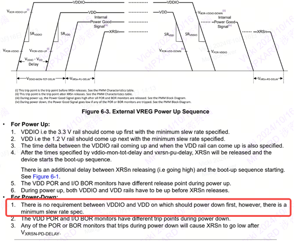
1. Power up and down timing requirements and slew rate requirements:


2.  Currently tested issues:
2.1  Power down timing is: 3.3V → 1.2V → XRSn
Impact assessment: According to the manual description, there are no special requirements for these two when power is turned off. Does it have to be risk-free?

2.2  Slew rate problem:
1)When Power on , Is there any risk if the voltage slew rate at 3.3V does not meet the specifications?
2)When Power off,  Is there any risk if the voltage slew rate does not meet the specifications at 3.3V and 1.2V?
  • Angela,

    I would refer to this section of the datasheet to give some needed background for the sections mentioned above:

    https://www.ti.com/document-viewer/TMS320F280039/datasheet#GUID-E311B1CE-8214-4C20-840B-DAF9E1F06EA8/GUID-3EC1BB52-69E9-4835-8374-8B9FD25AEFE4

    The assumption here is that VDD is monitored externally, so the goodness of VDD is not in question for the external VDD supply case.

    So for 2.1 there is no requirement, with the assumption that VDD is being monitored.  Else, the internal VDD POR trip point is too low to guarantee correct device operation until it is trigger and drives the XRSn low

    For 2.2:

    The risk on power up is if the rise time is too slow, then the BOR could release before the voltage has settled in the correct region.  Customer can refer to the timing delays along with the range for BOR release to determine if there is risk or not

    For power down I think same risk of being too slow, although it should be less risk than power up since BOR is fully functional.

    In both cases I think if there is too fast of a ramp there is risk of activating the ESD diodes in the device, and drawing excess current and/or latching up the IO buffer.

    For ramp rate on VDD, since again we have assumption there is external supervisor on this rail, it is more about a controlled power up seen by the device.

    Best,

    Matthew

  • 1. In conclusion:

    1.1  Power-up/down timing of 3.3V and 1.2V is not a problem;

    1.2  When Power-up/down ,slew rate of 3.3V and 1.2V  is a risk.  is it right?

    2. Solution:

    I have looked for many buck ICs, all of which have soft start function but do not meet the 3.3V slew rate; is there any good solution?
  • This is correct, can you give some the IC part numbers, just so I can take a look to see how far off we are from our spec?  We may have to use LDO based supply vs buck if this is more an issue with that topology.

    Best,

    Matthew

  • 1. The reason for the unsatisfactory slew rate is that :3.3V is generated by the front-stage buck, and the buck IC has a soft start function, which causes this problem. TPS562201 was selected, which has a 1ms soft start time

    2. I haven't found a buck IC without soft start function yet.

  • Dang,

    Can you comment which of the below startup graphs from the TPS562201 matches how you have implemented in the system?  Also, since these just show 1V for Vout; can you comment on what you see when configured for 3.3V Vout?  Is the power up time 3x shown below, or still 1ms?

    Best,
    Matthew

  • 1. I'm referring to the time at the arrow (TPS562201)

    2. The following is our measured waveform( CH1:3.3V)  has a relatively large delay time about 1 ms.

  • Dang,

    Thanks for the new info, this helps alot. 

    I think the VDD hold off is helping us here, to avoid an issue with the slower rise time of the VDDIO line. 

    Since the VDD is not coming on at all until ~2.85V it is also holding off XRSn during what might otherwise be an indeterminant time.  When it does come up, VDDIO is already within good range, such that the internal BOR monitor is stable/known good at this point as well.

    You can also see the XRSn line is not releasing until the expected range we have in the DS, which would also be an indication that things are not settled internally.

    If we believe that this relationship of VDDIO/VDD will hold I'm OK with the violation of the min slew rate, the device will come out of reset cleanly and operate correctly.

    Just curious, what is the source for VDD that holds off until VDDIO is almost done with its ramp?  

    Best,
    Matthew

  • I don't know what you're talking about。

    1. VDD is 1.2V, not 3.3V;

    2. VDDIO (3.3V)→LDO→ VDD (1.2V) 

  • I understand the  normal Power Up Sequence(Figure 6-3),but not solve my  current problems (eg. the waveforms that I display)

  • Dang,

    Let me give some more detail.

    The rise times listed in the DS are primarily to ensure that the internal POR/BOR monitoring circuit keeps the device in reset until the supplies are within spec.

    When VREGENz = 0V(not your use case), then the internal VREG supplies the 1.2V core supply and the goodness of that supply is the primary gate to the POR/BOR releasing reset.  In turn the ramp rate of that supply is all we are concerned with as well.

    However, when VREGENz= VDDIO(your use case), then 1.2V is also supplied externally and that also gates releasing reset.

    As you mentioned the VDDIO ramp from the BUCK is too slow/longer than the DS spec we give for VDDIO.  Normally, this would present a problem that the internal POR/BOR will release too soon before VDDIO is in range, and there could be risk that the device begins to execute code too early as well.

    However, based on your waveform, since VDD(1.2V) does not come active until VDDIO(3.3V) is at or near the 2.60V this is mitigating the slow ramp rate on VDDIO, holding off reset de-assertion correctly.  By the time the VDD rail does go high, the accurate VDDIO monitor is functioning within spec and we are gating reset correctly.

    So, even though we are in violation of the min ramp rate on VDDIO, due to how the VDD is applied I am OK waiving that requirement, because at the system level we are avoiding the potential condition a slow ramp on VDDIO would cause. 

    Basically, I think your current implementation will operate correctly after power up, so you can ignore the slow ramp on VDDIO/violation of the DS.

    Best,

    Matthew

  • “ However, based on your waveform, since VDD(1.2V) does not come active until VDDIO(3.3V) is at or near the 2.60V this is mitigating the slow ramp rate on VDDIO, holding off reset de-assertion correctly “

    why 2.6V is an  appropriate value ?

  • By 2.45V the more accurate BOR threshold has come online in the device, and will begin to monitor the VDDIO rail to drive XRSn pin correctly. Additionally there is ~120us after everything is detected "good" will continue to hold XRSn in case of any noise, etc.

    We can verify this "correct" by looking at the waveform you sent, you can see the XRSn doesn't start to rise until the DS listed voltage of ~2.81V.

    Best,

    Matthew

  • I couldn't find the source of 2.45V in the DS,  Only saw this
  • Dang,

    The 2.45V is not in the DS, by specifying the ramp rates of the VDDIO/VDD and how the internal POR/BOR is constructed we will make sure that the BOR is accurately monitoring the VDDIO rail before releasing XRSn.

    However, in your case, since VDD is held low and does not ramp with VDDIO we don't have to be as stringent on the ramp rate, as VDD being 0V will also guarantee that XRSn is held, even if VDDIO were in specification. 

    This was not a scenario we anticipated, which is why we only give ramp rates vs all the different turn on/working conditions of the different monitors inside the device.

    The ramp rates, coupled with the delays in the block diagram I posted earlier, will make sure the POR/BOR is not releasing reset too soon.

    Best,

    Matthew

  • So, just to confirm that  my current waveform is ok,right?
  • Yes, your provided waveform is showing the correct behavior for XRSn wrt to the voltages on VDDIO/VDD.  Device will come out of reset cleanly on a power up event.

    Best,

    Matthew

  • Another question:for power down , there are actual  test data and waveforms. Please help check if there is any problem.

    1. Test data


    2. Waveform

    CH1:3.3V CH3:1.2V CH2:RST

  • Dang,

    Apologies, this is acceptable for power down.  Since 1.2V is still good as VDDIO ramps down, device behavior is in known state when XRSn gets asserted(and stays asserted).  It looks like 3.3V and 1.2V ramp down together once 3.3V reaches that similar voltage range.

    Best,

    Matthew