This thread has been locked.

If you have a related question, please click the "Ask a related question" button in the top right corner. The newly created question will be automatically linked to this question.

TMS320F28379D: Configure EPWMs to load CMPA on SYNCIN

Part Number: TMS320F28379D
Other Parts Discussed in Thread: C2000WARE

Tool/software:

I am unable to configure the EPWMs to load CMPA on a SYNCIN event.

Here is my setup:

I'm using EPWM Modules 1 through 11. I need to load the shadowed CMPA and CMPB value for EPWMs 9 through 11 simultaneously for my design. Right now, I am attempting to do the following

- EPWM 1 configured to generate SYNCOUT pulse when TBCTR=0
- EPWM 2 through 11 configured to use SYNCOUT = SYNCIN
- EPWM 1 through 8 configured to be active high (not complementary)
- EPWM 9 through 11 configured to be active high complementary
- EPWM 9 through 11 configured to load CMPA and CMPB on SYNCIN


This last part is the the one that doesn't seem to work for me. 

I have attached a working test project that demonstrates the issue.

The relevant code is in lines 561-577

    EPwm9Regs.CMPCTL.bit.LOADAMODE = 0;
    EPwm9Regs.CMPCTL.bit.LOADASYNC = 2;

    EPwm9Regs.CMPCTL.bit.LOADBMODE = 0;
    EPwm9Regs.CMPCTL.bit.LOADBSYNC = 2;

    EPwm10Regs.CMPCTL.bit.LOADAMODE = 0;
    EPwm10Regs.CMPCTL.bit.LOADASYNC = 2;

    EPwm10Regs.CMPCTL.bit.LOADBMODE = 0;
    EPwm10Regs.CMPCTL.bit.LOADBSYNC = 2;

    EPwm11Regs.CMPCTL.bit.LOADAMODE = 0;
    EPwm11Regs.CMPCTL.bit.LOADASYNC = 2;

    EPwm11Regs.CMPCTL.bit.LOADBMODE = 0;
    EPwm11Regs.CMPCTL.bit.LOADBSYNC = 2;


When I run this program and test whether the PWM duty ratios are updating properly, I see that the duty ratio is never actually loaded, despite the fact that I can confirm the EPWM Sync signal is present.

Here is an image showing the PWM signals, sync signal output on a GPIO pin, and a flag that I'm using for triggering the measurement. The duty ratios should be different before and after the trigger point, but never change.


--------

For comparison, here is the behavior when I set EPwmxRegs.CMPCTL.bit.LOADASYNC = 0 for all three EPWMs. You can see that the duty ratios get updated at the CTR=0 point as they should.


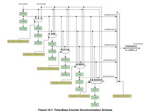
It seems I am missing some setting to get the EPWMs to load on sync, but I am unable to determine what is incorrect here. According to section 15.5 in the Technical Reference Manual I am setting all the CMPCTL registers properly.

Looking forward to hearing from you. I have attached a working project as a .zip file (please be sure to set the value of C2000WARE_ROOT properly in Project Properties > Linked Resources to ensure the library dependencies link properly) (EDIT Nov 22, 2024: project updated in comments)

Regards,
Rahul

  • Hi Rahul,

    Can you please double check that your Sync-IN source for those PWMs is set up correctly?

    Please send a snippet of the Sync select registers to verify that the sync source is set up correctly - if this is true, then the loading scheme should work if you have set up shadow load on sync.

    Best Regards,

    Allison

  • Hi Allison,

    I verified that the SYNCO TO SYNCI chain is functioning as I expect by connecting SYNCOs via the EXTSYNCOUT and OutputXBAR to a GPIO pin and probing with an oscilloscope.

    However, despite the SYNCI configuration, the CMPA/B load is not being triggered.

    Here are the settings copied from the configure_EPWM function in the project that I attached. 


    EALLOW;
    CpuSysRegs.PCLKCR0.bit.TBCLKSYNC = 0; // stop TBCTR incrementing
    EDIS;
    
    
    // EPWM 1
    EPwm1Regs.TBCTL.bit.CLKDIV = TB_DIV1; // CLKDIV=1 TBCLK=EPWMCLK/(HSPCLKDIV*CLKDIV)
    EPwm1Regs.TBCTL.bit.HSPCLKDIV = TB_DIV1; // HSPCLKDIV=1
    EPwm1Regs.TBCTL.bit.CTRMODE = TB_COUNT_UPDOWN; // Up-down mode
    
    EPwm1Regs.TBPRD = EPWM_TBPRD; // Counter period
    
    EPwm1Regs.CMPCTL.bit.SHDWAMODE = CC_SHADOW; // Shadow mode active for CMPA
    EPwm1Regs.CMPCTL.bit.SHDWBMODE = CC_SHADOW; // Shadow mode active for CMPB
    EPwm1Regs.CMPCTL.bit.LOADAMODE = CC_CTR_ZERO; // Load on TBCTR=TBPRD
    EPwm1Regs.CMPCTL.bit.LOADBMODE = CC_CTR_ZERO; // Load on TBCTR=TBPRD
    
    EPwm1Regs.CMPA.bit.CMPA = EPWM_TBPRD; // Initial value of CMPA
    
    EPwm1Regs.AQCTLA.bit.CAU = AQ_CLEAR; // Set EPWMA low on TBCTR=CMPA during up count
    EPwm1Regs.AQCTLA.bit.CAD = AQ_SET; // Set EPWMA high on TBCTR=CMPA during down count
    
    EPwm1Regs.TBCTL.bit.SYNCOSEL = TB_SYNC_IN; // Pass through SYNCIN signal (doesn't matter for what we're doing)
    EPwm1Regs.TBCTL.bit.PHSEN = TB_ENABLE; // Enable loading of PHS register on sync event
    // We will initially enable this so that we can force a sync to set up the phase shifts.
    // After forcing the sync, we will disable this.
    // Note: if this is enabled on EPWM1, the input X-BAR should be reconfigured to something
    // other than GPIO0 (otherwise TBCTR will be loaded with TBPHS when EPWM toggles)
    
    EPwm1Regs.TBPHS.bit.TBPHS = TBCTR_INIT_1; // load TBCTR with this value on phase load event to set up phase shifts between carriers
    EPwm1Regs.TBCTR = 0; // start counter with value of 0 (TBCTR will be written with TBPHS when we force a sync)
    EPwm1Regs.TBCTL.bit.PHSDIR = DIR_1; // some carriers will start counting up and some will start counting down
    // depending on their phase shifts
    
    EPwm1Regs.DBCTL.bit.POLSEL = DB_ACTV_HI; // this switch is shorted, so we don't invert the B channel
    EPwm1Regs.DBCTL.bit.OUT_MODE = DB_FULL_ENABLE; // Enable both falling and rising edge delays
    EPwm1Regs.DBFED.bit.DBFED = EPWM_DEADTIME; // Set delay for falling edge (DBFED)
    EPwm1Regs.DBRED.bit.DBRED = EPWM_DEADTIME; // Set delay for rising edge (DBRED)
    
    // EPWM 2
    EPwm2Regs.TBCTL.bit.CLKDIV = TB_DIV1; // CLKDIV=1 TBCLK=EPWMCLK/(HSPCLKDIV*CLKDIV)
    EPwm2Regs.TBCTL.bit.HSPCLKDIV = TB_DIV1; // HSPCLKDIV=1
    EPwm2Regs.TBCTL.bit.CTRMODE = TB_COUNT_UPDOWN; // Up-down mode
    
    EPwm2Regs.TBPRD = EPWM_TBPRD; // Counter period
    
    EPwm2Regs.CMPCTL.bit.SHDWAMODE = CC_SHADOW; // Shadow mode active for CMPA
    EPwm2Regs.CMPCTL.bit.SHDWBMODE = CC_SHADOW; // Shadow mode active for CMPB
    EPwm2Regs.CMPCTL.bit.LOADAMODE = CC_CTR_ZERO; // Load on TBCTR=TBPRD
    EPwm2Regs.CMPCTL.bit.LOADBMODE = CC_CTR_ZERO; // Load on TBCTR=TBPRD
    
    EPwm2Regs.CMPA.bit.CMPA = EPWM_TBPRD; // Initial value of CMPA
    
    EPwm2Regs.AQCTLA.bit.CAU = AQ_CLEAR; // Set EPWMA low on TBCTR=CMPA during up count
    EPwm2Regs.AQCTLA.bit.CAD = AQ_SET; // Set EPWMA high on TBCTR=CMPA during down count
    
    EPwm2Regs.TBCTL.bit.SYNCOSEL = TB_SYNC_IN; // Pass through SYNCIN signal (doesn't matter for what we're doing)
    EPwm2Regs.TBCTL.bit.PHSEN = TB_ENABLE; // Enable loading of PHS register on sync event
    // We will initially enable this so that we can force a sync to set up the phase shifts.
    // After forcing the sync, we will disable this.
    // Note: if this is enabled on EPWM1, the input X-BAR should be reconfigured to something
    // other than GPIO0 (otherwise TBCTR will be loaded with TBPHS when EPWM toggles)
    
    EPwm2Regs.TBPHS.bit.TBPHS = TBCTR_INIT_2; // load TBCTR with this value on phase load event to set up phase shifts between carriers
    EPwm2Regs.TBCTR = 0; // start counter with value of 0 (TBCTR will be written with TBPHS when we force a sync)
    EPwm2Regs.TBCTL.bit.PHSDIR = DIR_2; // some carriers will start counting up and some will start counting down
    // depending on their phase shifts
    
    EPwm2Regs.DBCTL.bit.POLSEL = DB_ACTV_HI; // Active high complementary - EPWMxB is inverted.
    EPwm2Regs.DBCTL.bit.OUT_MODE = DB_FULL_ENABLE; // Enable both falling and rising edge delays
    EPwm2Regs.DBFED.bit.DBFED = EPWM_DEADTIME; // Set delay for falling edge (DBFED)
    EPwm2Regs.DBRED.bit.DBRED = EPWM_DEADTIME; // Set delay for rising edge (DBRED)
    
    // EPWM 3
    EPwm3Regs.TBCTL.bit.CLKDIV = TB_DIV1; // CLKDIV=1 TBCLK=EPWMCLK/(HSPCLKDIV*CLKDIV)
    EPwm3Regs.TBCTL.bit.HSPCLKDIV = TB_DIV1; // HSPCLKDIV=1
    EPwm3Regs.TBCTL.bit.CTRMODE = TB_COUNT_UPDOWN; // Up-down mode
    
    EPwm3Regs.TBPRD = EPWM_TBPRD; // Counter period
    
    EPwm3Regs.CMPCTL.bit.SHDWAMODE = CC_SHADOW; // Shadow mode active for CMPA
    EPwm3Regs.CMPCTL.bit.SHDWBMODE = CC_SHADOW; // Shadow mode active for CMPB
    EPwm3Regs.CMPCTL.bit.LOADAMODE = CC_CTR_ZERO; // Load on TBCTR=TBPRD
    EPwm3Regs.CMPCTL.bit.LOADBMODE = CC_CTR_ZERO; // Load on TBCTR=TBPRD
    
    EPwm3Regs.CMPA.bit.CMPA = EPWM_TBPRD; // Initial value of CMPA
    
    EPwm3Regs.AQCTLA.bit.CAU = AQ_CLEAR; // Set EPWMA low on TBCTR=CMPA during up count
    EPwm3Regs.AQCTLA.bit.CAD = AQ_SET; // Set EPWMA high on TBCTR=CMPA during down count
    
    EPwm3Regs.TBCTL.bit.SYNCOSEL = TB_SYNC_IN; // Pass through SYNCIN signal (doesn't matter for what we're doing)
    EPwm3Regs.TBCTL.bit.PHSEN = TB_ENABLE; // Enable loading of PHS register on sync event
    // We will initially enable this so that we can force a sync to set up the phase shifts.
    // After forcing the sync, we will disable this.
    // Note: if this is enabled on EPWM1, the input X-BAR should be reconfigured to something
    // other than GPIO0 (otherwise TBCTR will be loaded with TBPHS when EPWM toggles)
    
    EPwm3Regs.TBPHS.bit.TBPHS = TBCTR_INIT_3; // load TBCTR with this value on phase load event to set up phase shifts between carriers
    EPwm3Regs.TBCTR = 0; // start counter with value of 0 (TBCTR will be written with TBPHS when we force a sync)
    EPwm3Regs.TBCTL.bit.PHSDIR = DIR_3; // some carriers will start counting up and some will start counting down
    // depending on their phase shifts
    
    EPwm3Regs.DBCTL.bit.POLSEL = DB_ACTV_HI; // Active high complementary - EPWMxB is inverted.
    EPwm3Regs.DBCTL.bit.OUT_MODE = DB_FULL_ENABLE; // Enable both falling and rising edge delays
    EPwm3Regs.DBFED.bit.DBFED = EPWM_DEADTIME; // Set delay for falling edge (DBFED)
    EPwm3Regs.DBRED.bit.DBRED = EPWM_DEADTIME; // Set delay for rising edge (DBRED)
    
    // EPWM 4
    EPwm4Regs.TBCTL.bit.CLKDIV = TB_DIV1; // CLKDIV=1 TBCLK=EPWMCLK/(HSPCLKDIV*CLKDIV)
    EPwm4Regs.TBCTL.bit.HSPCLKDIV = TB_DIV1; // HSPCLKDIV=1
    EPwm4Regs.TBCTL.bit.CTRMODE = TB_COUNT_UPDOWN; // Up-down mode
    
    EPwm4Regs.TBPRD = EPWM_TBPRD; // Counter period
    
    EPwm4Regs.CMPCTL.bit.SHDWAMODE = CC_SHADOW; // Shadow mode active for CMPA
    EPwm4Regs.CMPCTL.bit.SHDWBMODE = CC_SHADOW; // Shadow mode active for CMPB
    EPwm4Regs.CMPCTL.bit.LOADAMODE = CC_CTR_ZERO; // Load on TBCTR=TBPRD
    EPwm4Regs.CMPCTL.bit.LOADBMODE = CC_CTR_ZERO; // Load on TBCTR=TBPRD
    
    EPwm4Regs.CMPA.bit.CMPA = EPWM_TBPRD; // Initial value of CMPA
    
    EPwm4Regs.AQCTLA.bit.CAU = AQ_CLEAR; // Set EPWMA low on TBCTR=CMPA during up count
    EPwm4Regs.AQCTLA.bit.CAD = AQ_SET; // Set EPWMA high on TBCTR=CMPA during down count
    
    EPwm4Regs.TBCTL.bit.SYNCOSEL = TB_SYNC_IN; // Pass through SYNCIN signal (doesn't matter for what we're doing)
    EPwm4Regs.TBCTL.bit.PHSEN = TB_ENABLE; // Enable loading of PHS register on sync event
    // We will initially enable this so that we can force a sync to set up the phase shifts.
    // After forcing the sync, we will disable this.
    // Note: if this is enabled on EPWM1, the input X-BAR should be reconfigured to something
    // other than GPIO0 (otherwise TBCTR will be loaded with TBPHS when EPWM toggles)
    
    EPwm4Regs.TBPHS.bit.TBPHS = TBCTR_INIT_4; // load TBCTR with this value on phase load event to set up phase shifts between carriers
    EPwm4Regs.TBCTR = 0; // start counter with value of 0 (TBCTR will be written with TBPHS when we force a sync)
    EPwm4Regs.TBCTL.bit.PHSDIR = DIR_4; // some carriers will start counting up and some will start counting down
    // depending on their phase shifts
    
    EPwm4Regs.DBCTL.bit.POLSEL = DB_ACTV_HI; // Active high complementary - EPWMxB is inverted.
    EPwm4Regs.DBCTL.bit.OUT_MODE = DB_FULL_ENABLE; // Enable both falling and rising edge delays
    EPwm4Regs.DBFED.bit.DBFED = EPWM_DEADTIME; // Set delay for falling edge (DBFED)
    EPwm4Regs.DBRED.bit.DBRED = EPWM_DEADTIME; // Set delay for rising edge (DBRED)
    
    // EPWM 5
    EPwm5Regs.TBCTL.bit.CLKDIV = TB_DIV1; // CLKDIV=1 TBCLK=EPWMCLK/(HSPCLKDIV*CLKDIV)
    EPwm5Regs.TBCTL.bit.HSPCLKDIV = TB_DIV1; // HSPCLKDIV=1
    EPwm5Regs.TBCTL.bit.CTRMODE = TB_COUNT_UPDOWN; // Up-down mode
    
    EPwm5Regs.TBPRD = EPWM_TBPRD; // Counter period
    
    EPwm5Regs.CMPCTL.bit.SHDWAMODE = CC_SHADOW; // Shadow mode active for CMPA
    EPwm5Regs.CMPCTL.bit.SHDWBMODE = CC_SHADOW; // Shadow mode active for CMPB
    EPwm5Regs.CMPCTL.bit.LOADAMODE = CC_CTR_ZERO; // Load on TBCTR=TBPRD
    EPwm5Regs.CMPCTL.bit.LOADBMODE = CC_CTR_ZERO; // Load on TBCTR=TBPRD
    
    EPwm5Regs.CMPA.bit.CMPA = EPWM_TBPRD; // Initial value of CMPA
    
    EPwm5Regs.AQCTLA.bit.CAU = AQ_CLEAR; // Set EPWMA low on TBCTR=CMPA during up count
    EPwm5Regs.AQCTLA.bit.CAD = AQ_SET; // Set EPWMA high on TBCTR=CMPA during down count
    
    EPwm5Regs.TBCTL.bit.SYNCOSEL = TB_SYNC_IN; // Pass through SYNCIN signal (doesn't matter for what we're doing)
    EPwm5Regs.TBCTL.bit.PHSEN = TB_ENABLE; // Enable loading of PHS register on sync event
    // We will initially enable this so that we can force a sync to set up the phase shifts.
    // After forcing the sync, we will disable this.
    // Note: if this is enabled on EPWM1, the input X-BAR should be reconfigured to something
    // other than GPIO0 (otherwise TBCTR will be loaded with TBPHS when EPWM toggles)
    
    EPwm5Regs.TBPHS.bit.TBPHS = TBCTR_INIT_5; // load TBCTR with this value on phase load event to set up phase shifts between carriers
    EPwm5Regs.TBCTR = 0; // start counter with value of 0 (TBCTR will be written with TBPHS when we force a sync)
    EPwm5Regs.TBCTL.bit.PHSDIR = DIR_5; // some carriers will start counting up and some will start counting down
    // depending on their phase shifts
    
    EPwm5Regs.DBCTL.bit.POLSEL = DB_ACTV_HI; // Active high complementary - EPWMxB is inverted.
    EPwm5Regs.DBCTL.bit.OUT_MODE = DB_FULL_ENABLE; // Enable both falling and rising edge delays
    EPwm5Regs.DBFED.bit.DBFED = EPWM_DEADTIME; // Set delay for falling edge (DBFED)
    EPwm5Regs.DBRED.bit.DBRED = EPWM_DEADTIME; // Set delay for rising edge (DBRED)
    
    // EPWM 6
    EPwm6Regs.TBCTL.bit.CLKDIV = TB_DIV1; // CLKDIV=1 TBCLK=EPWMCLK/(HSPCLKDIV*CLKDIV)
    EPwm6Regs.TBCTL.bit.HSPCLKDIV = TB_DIV1; // HSPCLKDIV=1
    EPwm6Regs.TBCTL.bit.CTRMODE = TB_COUNT_UPDOWN; // Up-down mode
    
    EPwm6Regs.TBPRD = EPWM_TBPRD; // Counter period
    
    EPwm6Regs.CMPCTL.bit.SHDWAMODE = CC_SHADOW; // Shadow mode active for CMPA
    EPwm6Regs.CMPCTL.bit.SHDWBMODE = CC_SHADOW; // Shadow mode active for CMPB
    EPwm6Regs.CMPCTL.bit.LOADAMODE = CC_CTR_ZERO; // Load on TBCTR=TBPRD
    EPwm6Regs.CMPCTL.bit.LOADBMODE = CC_CTR_ZERO; // Load on TBCTR=TBPRD
    
    EPwm6Regs.CMPA.bit.CMPA = EPWM_TBPRD; // Initial value of CMPA
    
    EPwm6Regs.AQCTLA.bit.CAU = AQ_CLEAR; // Set EPWMA low on TBCTR=CMPA during up count
    EPwm6Regs.AQCTLA.bit.CAD = AQ_SET; // Set EPWMA high on TBCTR=CMPA during down count
    
    EPwm6Regs.TBCTL.bit.SYNCOSEL = TB_SYNC_IN; // Pass through SYNCIN signal (doesn't matter for what we're doing)
    EPwm6Regs.TBCTL.bit.PHSEN = TB_ENABLE; // Enable loading of PHS register on sync event
    // We will initially enable this so that we can force a sync to set up the phase shifts.
    // After forcing the sync, we will disable this.
    // Note: if this is enabled on EPWM1, the input X-BAR should be reconfigured to something
    // other than GPIO0 (otherwise TBCTR will be loaded with TBPHS when EPWM toggles)
    
    EPwm6Regs.TBPHS.bit.TBPHS = TBCTR_INIT_6; // load TBCTR with this value on phase load event to set up phase shifts between carriers
    EPwm6Regs.TBCTR = 0; // start counter with value of 0 (TBCTR will be written with TBPHS when we force a sync)
    EPwm6Regs.TBCTL.bit.PHSDIR = DIR_6; // some carriers will start counting up and some will start counting down
    // depending on their phase shifts
    
    EPwm6Regs.DBCTL.bit.POLSEL = DB_ACTV_HI; // Active high complementary - EPWMxB is inverted.
    EPwm6Regs.DBCTL.bit.OUT_MODE = DB_FULL_ENABLE; // Enable both falling and rising edge delays
    EPwm6Regs.DBFED.bit.DBFED = EPWM_DEADTIME; // Set delay for falling edge (DBFED)
    EPwm6Regs.DBRED.bit.DBRED = EPWM_DEADTIME; // Set delay for rising edge (DBRED)
    
    // EPWM 7
    EPwm7Regs.TBCTL.bit.CLKDIV = TB_DIV1; // CLKDIV=1 TBCLK=EPWMCLK/(HSPCLKDIV*CLKDIV)
    EPwm7Regs.TBCTL.bit.HSPCLKDIV = TB_DIV1; // HSPCLKDIV=1
    EPwm7Regs.TBCTL.bit.CTRMODE = TB_COUNT_UPDOWN; // Up-down mode
    
    EPwm7Regs.TBPRD = EPWM_TBPRD; // Counter period
    
    EPwm7Regs.CMPCTL.bit.SHDWAMODE = CC_SHADOW; // Shadow mode active for CMPA
    EPwm7Regs.CMPCTL.bit.SHDWBMODE = CC_SHADOW; // Shadow mode active for CMPB
    EPwm7Regs.CMPCTL.bit.LOADAMODE = CC_CTR_ZERO; // Load on TBCTR=TBPRD
    EPwm7Regs.CMPCTL.bit.LOADBMODE = CC_CTR_ZERO; // Load on TBCTR=TBPRD
    
    EPwm7Regs.CMPA.bit.CMPA = EPWM_TBPRD; // Initial value of CMPA
    
    EPwm7Regs.AQCTLA.bit.CAU = AQ_CLEAR; // Set EPWMA low on TBCTR=CMPA during up count
    EPwm7Regs.AQCTLA.bit.CAD = AQ_SET; // Set EPWMA high on TBCTR=CMPA during down count
    
    EPwm7Regs.TBCTL.bit.SYNCOSEL = TB_SYNC_IN; // Pass through SYNCIN signal (doesn't matter for what we're doing)
    EPwm7Regs.TBCTL.bit.PHSEN = TB_ENABLE; // Enable loading of PHS register on sync event
    // We will initially enable this so that we can force a sync to set up the phase shifts.
    // After forcing the sync, we will disable this.
    // Note: if this is enabled on EPWM1, the input X-BAR should be reconfigured to something
    // other than GPIO0 (otherwise TBCTR will be loaded with TBPHS when EPWM toggles)
    
    EPwm7Regs.TBPHS.bit.TBPHS = TBCTR_INIT_7; // load TBCTR with this value on phase load event to set up phase shifts between carriers
    EPwm7Regs.TBCTR = 0; // start counter with value of 0 (TBCTR will be written with TBPHS when we force a sync)
    EPwm7Regs.TBCTL.bit.PHSDIR = DIR_7; // some carriers will start counting up and some will start counting down
    // depending on their phase shifts
    
    EPwm7Regs.DBCTL.bit.POLSEL = DB_ACTV_HI; // Active high complementary - EPWMxB is inverted.
    EPwm7Regs.DBCTL.bit.OUT_MODE = DB_FULL_ENABLE; // Enable both falling and rising edge delays
    EPwm7Regs.DBFED.bit.DBFED = EPWM_DEADTIME; // Set delay for falling edge (DBFED)
    EPwm7Regs.DBRED.bit.DBRED = EPWM_DEADTIME; // Set delay for rising edge (DBRED)
    
    // EPWM 8
    EPwm8Regs.TBCTL.bit.CLKDIV = TB_DIV1; // CLKDIV=1 TBCLK=EPWMCLK/(HSPCLKDIV*CLKDIV)
    EPwm8Regs.TBCTL.bit.HSPCLKDIV = TB_DIV1; // HSPCLKDIV=1
    EPwm8Regs.TBCTL.bit.CTRMODE = TB_COUNT_UPDOWN; // Up-down mode
    
    EPwm8Regs.TBPRD = EPWM_TBPRD; // Counter period
    
    EPwm8Regs.CMPCTL.bit.SHDWAMODE = CC_SHADOW; // Shadow mode active for CMPA
    EPwm8Regs.CMPCTL.bit.SHDWBMODE = CC_SHADOW; // Shadow mode active for CMPB
    EPwm8Regs.CMPCTL.bit.LOADAMODE = CC_CTR_ZERO; // Load on TBCTR=TBPRD
    EPwm8Regs.CMPCTL.bit.LOADBMODE = CC_CTR_ZERO; // Load on TBCTR=TBPRD
    
    EPwm8Regs.CMPA.bit.CMPA = EPWM_TBPRD; // Initial value of CMPA
    
    EPwm8Regs.AQCTLA.bit.CAU = AQ_CLEAR; // Set EPWMA low on TBCTR=CMPA during up count
    EPwm8Regs.AQCTLA.bit.CAD = AQ_SET; // Set EPWMA high on TBCTR=CMPA during down count
    
    EPwm8Regs.TBCTL.bit.SYNCOSEL = TB_SYNC_IN; // Pass through SYNCIN signal (doesn't matter for what we're doing)
    EPwm8Regs.TBCTL.bit.PHSEN = TB_ENABLE; // Enable loading of PHS register on sync event
    // We will initially enable this so that we can force a sync to set up the phase shifts.
    // After forcing the sync, we will disable this.
    // Note: if this is enabled on EPWM1, the input X-BAR should be reconfigured to something
    // other than GPIO0 (otherwise TBCTR will be loaded with TBPHS when EPWM toggles)
    
    EPwm8Regs.TBPHS.bit.TBPHS = TBCTR_INIT_8; // load TBCTR with this value on phase load event to set up phase shifts between carriers
    EPwm8Regs.TBCTR = 0; // start counter with value of 0 (TBCTR will be written with TBPHS when we force a sync)
    EPwm8Regs.TBCTL.bit.PHSDIR = DIR_8; // some carriers will start counting up and some will start counting down
    // depending on their phase shifts
    
    EPwm8Regs.DBCTL.bit.POLSEL = DB_ACTV_HI; // Active high complementary - EPWMxB is inverted.
    EPwm8Regs.DBCTL.bit.OUT_MODE = DB_FULL_ENABLE; // Enable both falling and rising edge delays
    EPwm8Regs.DBFED.bit.DBFED = EPWM_DEADTIME; // Set delay for falling edge (DBFED)
    EPwm8Regs.DBRED.bit.DBRED = EPWM_DEADTIME; // Set delay for rising edge (DBRED)
    
    // EPWM 9
    EPwm9Regs.TBCTL.bit.CLKDIV = TB_DIV1; // CLKDIV=1 TBCLK=EPWMCLK/(HSPCLKDIV*CLKDIV)
    EPwm9Regs.TBCTL.bit.HSPCLKDIV = TB_DIV1; // HSPCLKDIV=1
    EPwm9Regs.TBCTL.bit.CTRMODE = TB_COUNT_UPDOWN; // Up-down mode
    
    EPwm9Regs.TBPRD = EPWM_TBPRD; // Counter period
    
    EPwm9Regs.CMPCTL.bit.SHDWAMODE = CC_SHADOW; // Shadow mode active for CMPA
    EPwm9Regs.CMPCTL.bit.SHDWBMODE = CC_SHADOW; // Shadow mode active for CMPB
    EPwm9Regs.CMPCTL.bit.LOADAMODE = CC_CTR_ZERO; // Load on TBCTR=TBPRD
    EPwm9Regs.CMPCTL.bit.LOADBMODE = CC_CTR_ZERO; // Load on TBCTR=TBPRD
    
    EPwm9Regs.CMPA.bit.CMPA = EPWM_CMP_INIT; // Initial value of CMPA
    
    EPwm9Regs.AQCTLA.bit.CAU = AQ_CLEAR; // Set EPWMA low on TBCTR=CMPA during up count
    EPwm9Regs.AQCTLA.bit.CAD = AQ_SET; // Set EPWMA high on TBCTR=CMPA during down count
    
    EPwm9Regs.TBCTL.bit.SYNCOSEL = TB_SYNC_IN; // Pass through SYNCIN signal (doesn't matter for what we're doing)
    EPwm9Regs.TBCTL.bit.PHSEN = TB_ENABLE; // Enable loading of PHS register on sync event
    // We will initially enable this so that we can force a sync to set up the phase shifts.
    // After forcing the sync, we will disable this.
    // Note: if this is enabled on EPWM1, the input X-BAR should be reconfigured to something
    // other than GPIO0 (otherwise TBCTR will be loaded with TBPHS when EPWM toggles)
    
    EPwm9Regs.TBPHS.bit.TBPHS = TBCTR_INIT_9; // load TBCTR with this value on phase load event to set up phase shifts between carriers
    EPwm9Regs.TBCTR = 0; // start counter with value of 0 (TBCTR will be written with TBPHS when we force a sync)
    EPwm9Regs.TBCTL.bit.PHSDIR = DIR_9; // some carriers will start counting up and some will start counting down
    // depending on their phase shifts
    
    EPwm9Regs.DBCTL.bit.POLSEL = DB_ACTV_HIC; // Active high complementary - EPWMxB is inverted.
    EPwm9Regs.DBCTL.bit.OUT_MODE = DB_FULL_ENABLE; // Enable both falling and rising edge delays
    EPwm9Regs.DBFED.bit.DBFED = EPWM_DEADTIME; // Set delay for falling edge (DBFED)
    EPwm9Regs.DBRED.bit.DBRED = EPWM_DEADTIME; // Set delay for rising edge (DBRED)
    
    // EPWM 10
    EPwm10Regs.TBCTL.bit.CLKDIV = TB_DIV1; // CLKDIV=1 TBCLK=EPWMCLK/(HSPCLKDIV*CLKDIV)
    EPwm10Regs.TBCTL.bit.HSPCLKDIV = TB_DIV1; // HSPCLKDIV=1
    EPwm10Regs.TBCTL.bit.CTRMODE = TB_COUNT_UPDOWN; // Up-down mode
    
    EPwm10Regs.TBPRD = EPWM_TBPRD; // Counter period
    
    EPwm10Regs.CMPCTL.bit.SHDWAMODE = CC_SHADOW; // Shadow mode active for CMPA
    EPwm10Regs.CMPCTL.bit.SHDWBMODE = CC_SHADOW; // Shadow mode active for CMPB
    EPwm10Regs.CMPCTL.bit.LOADAMODE = CC_CTR_ZERO; // Load on TBCTR=TBPRD
    EPwm10Regs.CMPCTL.bit.LOADBMODE = CC_CTR_ZERO; // Load on TBCTR=TBPRD
    
    EPwm10Regs.CMPA.bit.CMPA = EPWM_CMP_INIT; // Initial value of CMPA
    
    EPwm10Regs.AQCTLA.bit.CAU = AQ_CLEAR; // Set EPWMA low on TBCTR=CMPA during up count
    EPwm10Regs.AQCTLA.bit.CAD = AQ_SET; // Set EPWMA high on TBCTR=CMPA during down count
    
    EPwm10Regs.TBCTL.bit.SYNCOSEL = TB_SYNC_IN; // Pass through SYNCIN signal (doesn't matter for what we're doing)
    EPwm10Regs.TBCTL.bit.PHSEN = TB_ENABLE; // Enable loading of PHS register on sync event
    // We will initially enable this so that we can force a sync to set up the phase shifts.
    // After forcing the sync, we will disable this.
    // Note: if this is enabled on EPWM1, the input X-BAR should be reconfigured to something
    // other than GPIO0 (otherwise TBCTR will be loaded with TBPHS when EPWM toggles)
    
    EPwm10Regs.TBPHS.bit.TBPHS = TBCTR_INIT_10; // load TBCTR with this value on phase load event to set up phase shifts between carriers
    EPwm10Regs.TBCTR = 0; // start counter with value of 0 (TBCTR will be written with TBPHS when we force a sync)
    EPwm10Regs.TBCTL.bit.PHSDIR = DIR_10; // some carriers will start counting up and some will start counting down
    // depending on their phase shifts
    
    EPwm10Regs.DBCTL.bit.POLSEL = DB_ACTV_HIC; // Active high complementary - EPWMxB is inverted.
    EPwm10Regs.DBCTL.bit.OUT_MODE = DB_FULL_ENABLE; // Enable both falling and rising edge delays
    EPwm10Regs.DBFED.bit.DBFED = EPWM_DEADTIME; // Set delay for falling edge (DBFED)
    EPwm10Regs.DBRED.bit.DBRED = EPWM_DEADTIME; // Set delay for rising edge (DBRED)
    
    // EPWM 11
    EPwm11Regs.TBCTL.bit.CLKDIV = TB_DIV1; // CLKDIV=1 TBCLK=EPWMCLK/(HSPCLKDIV*CLKDIV)
    EPwm11Regs.TBCTL.bit.HSPCLKDIV = TB_DIV1; // HSPCLKDIV=1
    EPwm11Regs.TBCTL.bit.CTRMODE = TB_COUNT_UPDOWN; // Up-down mode
    
    EPwm11Regs.TBPRD = EPWM_TBPRD; // Counter period
    
    EPwm11Regs.CMPCTL.bit.SHDWAMODE = CC_SHADOW; // Shadow mode active for CMPA
    EPwm11Regs.CMPCTL.bit.SHDWBMODE = CC_SHADOW; // Shadow mode active for CMPB
    EPwm11Regs.CMPCTL.bit.LOADAMODE = CC_CTR_ZERO; // Load on TBCTR=TBPRD
    EPwm11Regs.CMPCTL.bit.LOADBMODE = CC_CTR_ZERO; // Load on TBCTR=TBPRD
    
    EPwm11Regs.CMPA.bit.CMPA = EPWM_CMP_INIT; // Initial value of CMPA
    
    EPwm11Regs.AQCTLA.bit.CAU = AQ_CLEAR; // Set EPWMA low on TBCTR=CMPA during up count
    EPwm11Regs.AQCTLA.bit.CAD = AQ_SET; // Set EPWMA high on TBCTR=CMPA during down count
    
    EPwm11Regs.TBCTL.bit.SYNCOSEL = TB_SYNC_IN; // Pass through SYNCIN signal (doesn't matter for what we're doing)
    EPwm11Regs.TBCTL.bit.PHSEN = TB_ENABLE; // Enable loading of PHS register on sync event
    // We will initially enable this so that we can force a sync to set up the phase shifts.
    // After forcing the sync, we will disable this.
    // Note: if this is enabled on EPWM1, the input X-BAR should be reconfigured to something
    // other than GPIO0 (otherwise TBCTR will be loaded with TBPHS when EPWM toggles)
    
    EPwm11Regs.TBPHS.bit.TBPHS = TBCTR_INIT_11; // load TBCTR with this value on phase load event to set up phase shifts between carriers
    EPwm11Regs.TBCTR = 0; // start counter with value of 0 (TBCTR will be written with TBPHS when we force a sync)
    EPwm11Regs.TBCTL.bit.PHSDIR = DIR_11; // some carriers will start counting up and some will start counting down
    // depending on their phase shifts
    
    EPwm11Regs.DBCTL.bit.POLSEL = DB_ACTV_HIC; // Active high complementary - EPWMxB is inverted.
    EPwm11Regs.DBCTL.bit.OUT_MODE = DB_FULL_ENABLE; // Enable both falling and rising edge delays
    EPwm11Regs.DBFED.bit.DBFED = EPWM_DEADTIME; // Set delay for falling edge (DBFED)
    EPwm11Regs.DBRED.bit.DBRED = EPWM_DEADTIME; // Set delay for rising edge (DBRED)
    
    // setting the trip zone registers
    // we will use the trip zone to short out the upper 8 pairs of switches to use the 12-level hardware as a 4-Level
    EALLOW;
    
    EPwm9Regs.TZCTL.bit.TZA = TZ_FORCE_LO; // Set EPWMA high when the trip-zone is triggered
    EPwm9Regs.TZCTL.bit.TZB = TZ_FORCE_LO; // Set EPWMB high when the trip-zone is triggered
    EPwm9Regs.TZSEL.bit.OSHT1 = 1; // Enable TZ1 as a one-shot TZ event source
    EPwm9Regs.TZEINT.bit.OST = 0; // Enable TZ interrupt
    EPwm9Regs.TZCLR.bit.OST = 1; // Clear OST flag
    
    EPwm10Regs.TZCTL.bit.TZA = TZ_FORCE_LO; // Set EPWMA high when the trip-zone is triggered
    EPwm10Regs.TZCTL.bit.TZB = TZ_FORCE_LO; // Set EPWMB high when the trip-zone is triggered
    EPwm10Regs.TZSEL.bit.OSHT1 = 1; // Enable TZ1 as a one-shot TZ event source
    EPwm10Regs.TZEINT.bit.OST = 0; // Enable TZ interrupt
    EPwm10Regs.TZCLR.bit.OST = 1; // Clear OST flag
    
    EPwm11Regs.TZCTL.bit.TZA = TZ_FORCE_LO; // Set EPWMA high when the trip-zone is triggered
    EPwm11Regs.TZCTL.bit.TZB = TZ_FORCE_LO; // Set EPWMB high when the trip-zone is triggered
    EPwm11Regs.TZSEL.bit.OSHT1 = 1; // Enable TZ1 as a one-shot TZ event source
    EPwm11Regs.TZEINT.bit.OST = 0; // Enable TZ interrupt
    EPwm11Regs.TZCLR.bit.OST = 1; // Clear OST flag
    
    EDIS;
    
    // configure EPWMs to load CMPA and CMPB only when a sync is received
    
    EPwm9Regs.CMPCTL.bit.LOADAMODE = 0;
    EPwm9Regs.CMPCTL.bit.LOADASYNC = 2;
    
    EPwm9Regs.CMPCTL.bit.LOADBMODE = 0;
    EPwm9Regs.CMPCTL.bit.LOADBSYNC = 2;
    
    EPwm10Regs.CMPCTL.bit.LOADAMODE = 0;
    EPwm10Regs.CMPCTL.bit.LOADASYNC = 2;
    
    EPwm10Regs.CMPCTL.bit.LOADBMODE = 0;
    EPwm10Regs.CMPCTL.bit.LOADBSYNC = 2;
    
    EPwm11Regs.CMPCTL.bit.LOADAMODE = 0;
    EPwm11Regs.CMPCTL.bit.LOADASYNC = 2;
    
    EPwm11Regs.CMPCTL.bit.LOADBMODE = 0;
    EPwm11Regs.CMPCTL.bit.LOADBSYNC = 2;
    
    // SOC trigger for sampling
    EPwm1Regs.ETSEL.bit.SOCASEL = ET_CTR_ZERO; // ADCSOCA on TBCTR=TBPRD
    EPwm1Regs.ETPS.bit.SOCAPRD = 1; // Generate SOCA on 1st event
    EPwm1Regs.ETSEL.bit.SOCAEN = 1; // Enable SOCA generation
    
    // set up PWM1 interrupt for main control loop
    EPwm1Regs.ETSEL.bit.INTSEL = ET_CTR_ZERO; // Select INT on TBPRD event
    EPwm1Regs.ETSEL.bit.INTEN = 0; // Disable INT
    EPwm1Regs.ETPS.bit.INTPRD = 1; // Generate INT on 1st event
    EPwm1Regs.ETCLR.bit.INT = 1; // Clear interrupt flag
    
    /*
    * EPWM signals propagate via a daisy chain depicted in TRM section 15.4.3.3
    * According to the TRM, the longest daisy chain propagation path must not exceed four EPWM modules.
    * If necessary, the sync chain can be modified with appropriate settings of bits in SyncSocRegs.SYNCSELECT
    *
    * However, in practice, it is unclear how many modules can be chained before the syncin->syncout pulse propagation delay is]
    * greater than 1 EPWMCLK.
    *
    * To set sync phase shifts properly, we need to modify the default EXTSYNC1 setup such that it does not interfere with the SWFSYNC
    * that we use to sync all the modules.
    *
    * By default, EXTSYNC1 is connected to INPUT5 on the Input XBAR, and INPUT5 is connected to GPIO0 which we are using for EPWM1A.
    *
    * SWFSYNC and the synchronization input signal EPWMxSYNCI both trigger EPWM sync (TRM section 15.4.3.3 and Fig. 15-5).
    * Leaving the default value for EXTSYNC1 can cause improper phase alignment if a rising edge on EPWM1 occurs before PHSEN is disabled
    * (for example if this routine is interrupted between the SWFSYNC = 1 and PHSEN = 0 operations). To ensure reliable phase alignment,
    * we will connect INPUT5 on the Input XBAR to an unused GPIO pin such that the only synchronizing signal is the SWFSYNC.
    */
    
    /*
    * EPWM sync triggers are latched until TBCTR is loaded with the value of TBPHS on the next TBCLK edge (TRM section 15.4.3.3)
    * Using SWFSYNC to synchronize a chain while TBCLKs are incrementing will result in a delay of TBCLK between the first EPWM module
    * in the chain and the subsequent ones, as the SYNCOUT signal only results in a synchronization at the next TBCLK edge.
    *
    * Therefore, when possible, the SWFSYNC should be set (and consequently latched) before the TBCLKSYNC bit is set to 1.
    */
    
    EALLOW;
    InputXbarRegs.INPUT1SELECT = 26; // route INPUT1 to GPIO 26 that we will use exclusively for tripping PWMs
    InputXbarRegs.INPUT5SELECT = 25; // route INPUT5 to an unused GPIO pin to not interfere with EXTSYNC1
    EDIS;
    
    EALLOW;
    EPwm1Regs.TBCTL.bit.SWFSYNC = 1; // force synchronization of EPWMs in chain starting with EPWM1
    CpuSysRegs.PCLKCR0.bit.TBCLKSYNC = 1; // start all TBCTR incrementing
    
    EPwm1Regs.TBCTL.bit.PHSEN = TB_DISABLE; // turn off PHSEN for all EPWMs to prevent subsequent phase loading
    EPwm2Regs.TBCTL.bit.PHSEN = TB_DISABLE;
    EPwm3Regs.TBCTL.bit.PHSEN = TB_DISABLE;
    EPwm4Regs.TBCTL.bit.PHSEN = TB_DISABLE;
    EPwm5Regs.TBCTL.bit.PHSEN = TB_DISABLE;
    EPwm6Regs.TBCTL.bit.PHSEN = TB_DISABLE;
    EPwm7Regs.TBCTL.bit.PHSEN = TB_DISABLE;
    EPwm8Regs.TBCTL.bit.PHSEN = TB_DISABLE;
    EPwm9Regs.TBCTL.bit.PHSEN = TB_DISABLE;
    EPwm10Regs.TBCTL.bit.PHSEN = TB_DISABLE;
    EPwm11Regs.TBCTL.bit.PHSEN = TB_DISABLE;
    
    
    EDIS;
    
    EALLOW;
    
    EPwm1Regs.TBCTL.bit.SYNCOSEL = 3; // SYNCOSEL for EPWM1 on CTR = 0
    EPwm1Regs.TBCTL2.bit.SYNCOSELX = 1;
    EPwm1Regs.CMPC = 0;
    
    SyncSocRegs.SYNCSELECT.bit.EPWM4SYNCIN = 0; // these are the default values
    SyncSocRegs.SYNCSELECT.bit.EPWM7SYNCIN = 0;
    SyncSocRegs.SYNCSELECT.bit.EPWM10SYNCIN = 0;
    SyncSocRegs.SYNCSELECT.bit.SYNCOUT = 0;
    
    // see TRM 9.4 for where these settings come from
    // we will use Output 1 on the Output XBAR
    OutputXbarRegs.OUTPUT1MUX0TO15CFG.bit.MUX14 = 3; // select EXTSYNCOUT in its corresponding mux (see TRM Table 9.4)
    OutputXbarRegs.OUTPUT1MUXENABLE.bit.MUX14 = 1; // enable OUTPUT1
    
    EDIS;

  • Hi Rahul,

    Thanks for the information. Please give me another few days to take a look.

    Best Regards,

    Allison

  • Hi Allison,

    Thanks. Looking forward to hearing back from you and/or anyone else on the C2000 team.

    Regards,
    Rahul

  • Hi Rahul,

    No update yet- I will follow up tomorrow. Appreciate the patience!

    Best Regards,

    Allison

  • Hi ,

    After extensive trial and error, I have determined that the way to get CMPA to load on SYNCI is to set

    EPwmxRegs.TBCTL.bit.PHSEN = 1 

    In other words, the PHSEN bit does more than just loading TBCTR with the value of TBPHS on sync, it also appears to gate whether CMPA gets loaded on sync.

    There's no mention of this anywhere in the Technical Reference Manual. I'd like to understand whether this is indeed the way PHSEN is designed to operate within the EPWM module or if it only works in this project by some coincidence.

    I have attached a new zip file that can be A/B tested to verify this behavior.

    3187.test_epwm_sync.zip

    Here, lines 645 to 655 are commented out and because PHSEN is set to 1 for all modules, the CMPA load on SYNCI behavior is as expected.

    If you uncomment these lines (set PHSEN = 0 for all modules) the loading no longer works.

    Best,
    Rahul

  • Hi Rahul,

    Appreciate the perseverance- glad you were able to get the desired output.

    The PHSEN bit will determine whether the sync pulse is able to be used as a SYNC-IN source for the PWM, so this behavior aligns with the TRM when it mentions "Clearing the TBCTL[PHSEN] bit configures the ePWM to ignore the synchronization input pulse." The SYNC-IN pulse is what is used for the loading strobe.

    However, it may not be clear in regard the SYNC signal being used for other register loading (beyond TBPHS). I will make a note for this to be clarified in this section in the future Slight smile

    Best Regards,

    Allison

  • Hi Allison,

    Appreciate the note to clarify this in the future. I interpreted the statement you're referring to about TBCTL as only applying to the TB submodule, not CC also. It appears from the explanation that TBCTL[PHSEN] configures all submodules within the EPWM module to ignore the SYNCIN pulse. 

    Best,
    Rahul