This thread has been locked.

If you have a related question, please click the "Ask a related question" button in the top right corner. The newly created question will be automatically linked to this question.

TMS320F28P550SJ: Crystal oscillator circuit for F28P550 design

Part Number: TMS320F28P550SJ

Tool/software:

Looking at TI designs for F28P550XJ I see some differences between the design of the Control Card and the Launchpad on the Crystal Oscillator circuit.

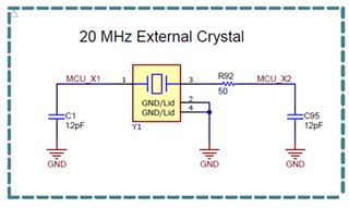
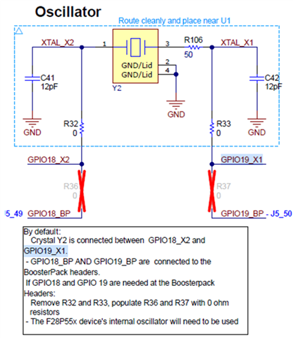
On the Control Card the dampening resistor is shown to be connected on MCU_X2 (R92) which is defined as “Crystal oscillator output”, while on the Launchpad design is shown to be connected on GPIO19_X1 (R106), which is defined as “Crystal oscillator input”.

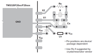
 Moreover, in some other TI documents about the Hardware Design Guidelines the following PCB layout is recommended, where the dampening resistor (Rs) is connected on X2 path, as can be seen below:


The questions that arise here is where the dampening resistor should be connected, on X1 path or X2 path? How would the two different connections affect the clock signal going into the DSC and overall, the quality of the design?

 Below you can see the crystal oscillator circuit for each design:

Control Card design (from sprr500) Launchpad Design (from sprr499)

Thanks!

  • Hello, 

    The correct answer for dampening resistor is in datasheet you shared (Hardware Design Guidelines for TMS320F28xx and TMS320F28xxx DSCs) https://www.ti.com/lit/an/spraas1d/spraas1d.pdf, page 25. Please connect dampening resistor to the crystal output (X2). 

  • I agree with the resolution, actually I believe is wrong to have the dampening resistor in X1 path. Does anyone know what the effect of having the resistor on X1 path, would be? I would say that rise and fall time would be increased, depending on the X1 input capacitance. I was also wondering if anyone at TI have measured the rise and fall time for both designs, control card and launchpad.

  • Hello, 

    You can find crystal characterization for Control card in this pdf report: file:

     TI+TMDSCNCD28P55X+PCB+Evaluation+Report+49+050224.pdf

    Placing the resistor on X1 will influence the input drive level and potentially reduce the gain of the oscillator's amplification stage. By reducing the drive level to the crystal, the risk of overdriving and damaging crystal can be reduced. 

    Placing it on the X2 will stabilize the oscillator by reducing harmonic distortion and ensure the crystal operates at its fundamental frequency. TI recommends putting resistor on X2. There were not any issues on LaunchPad crystal so far, but the note will be added to suggest connection to X2.

  • Thank you Stevan, this was really helpful!