


Tool/software:
Note: Update for CCSv20.2.0. This page will continue to be updated as necessary for relevant information to the FAQ.
Question: Where are the Flash Settings for my device in CCS?
Answer: In order to reach the Flash Settings, proceed with the following steps:
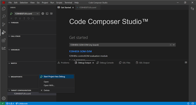
- Connect to the device by right-clicking the Target Configuration ccxml for your device and select ‘Start Project-less Debug’.
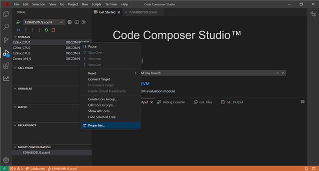
- Right-Click the CPU target thread for your device and select the ‘Connect Target’ option.
- Right-click the CPU target thread and scroll down to select the ‘Properties’ tab.
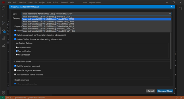
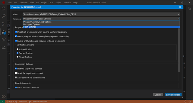
- A dialog box will appear showing the current device core and CCS category. Select the ‘Category’ option and click on the option listed as ‘Flash Settings’.
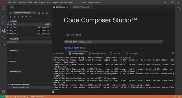
Question: Where can I find debug information output?
Answer: Debug programming messages can be found in the Debug Output tab in the CCS Interface. In order to enable verbose output, select the ‘Enable Verbose Output’ checkbox at the end of the Flash Settings dialog box.
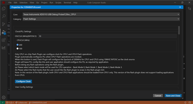
Question: What are the possible clock settings for my device?
Answer: Available CPU clock settings exist for 200MHz and 100Mhz, using 10MHz INTOSC as the clock source.
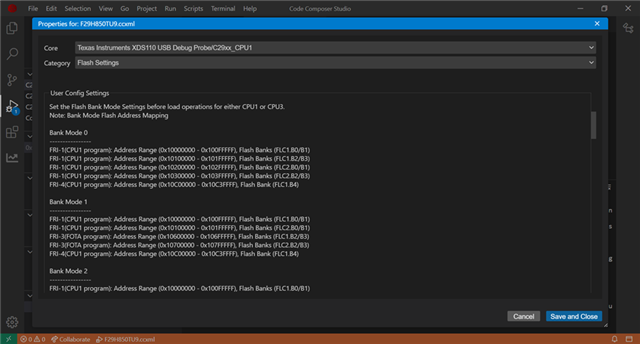
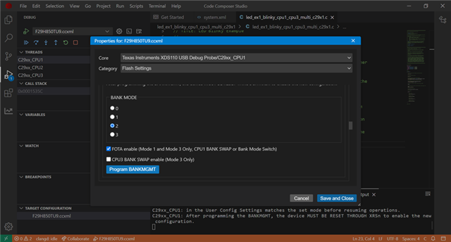
Question: What are the User Config Settings within Flash Settings category?
Answer: The User Config Settings for the devices provides information for the Flash Bank Mode Settings before load operations for either CPU1 or CPU3. A CPU configuration map is provided per bank mode and details the flash read-interface (FRI) used with the associated CPU core. When switching between Bank Modes, select the desired bank mode.
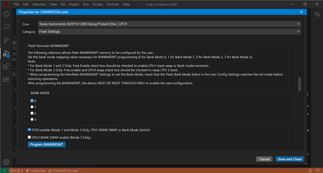
Question: What is Flash Nonmain BANKMGMT?
Answer: Flash NonMain BANKMGMT is a user configurable option for bank mode selection. Once the Bank Mode value is selected, the user has the option to program BANKMGMT. For F29x devices, Bank Mode 0 is the default. After BANKMGMT has been programmed, the user must issue a Device XRSn/Power-On Reset for the new BANKMGMT value to take effect. FOTA Programming is capable in Bank Mode 1 and Bank Mode 3 only.
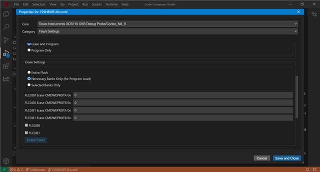
Question: What options for programming are in Download Settings?
Answer: Download Settings has several useful options for programming. Before a flash programming operation begins, users have the option to select ‘Reset target before flash programming/operations’. The ‘Allow Flash RAMOPEN’ feature provides a way for bootloader applications to have exclusive access to RAM for the purpose of storing code or data downloaded from an external source (for more details, consult the Technical Reference Manual). Program protections are provided per bank and can be enabled by the user.
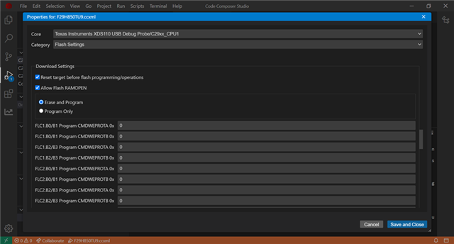
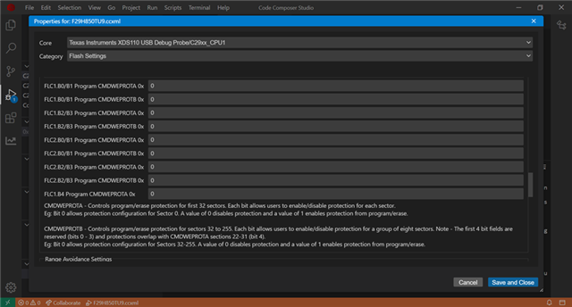
Question: How can I set the protections for Flash Programming?
Answer: Flash programming protections can be set by enabling/disabling the Flash Controller CMDWEPROT variable on a per bank basis. CMDWEPROTA controls program/erase for the first 32 sectors, and CMDWEPROTB controls program/erase for sectors 32 to 255. A value of 0 disables protection and a value of 1 enables protection from program/erase.
Question: How can I avoid programming a section of Flash?
Answer: During program load, a given range can be avoided during programming by using the ‘Enable Range Avoidance’ checkbox and setting an appropriate memory range.
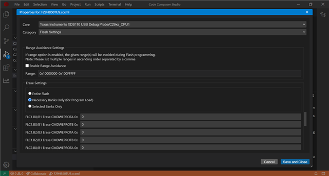
Question: I’m unable to load both CPU1 and CPU3 flash applications using the Flash Plugin with CPU1 core.
Answer: In the Erase Settings configuration selection, make sure that you have selected “Necessary Banks Only (for Program Load)” as your option.
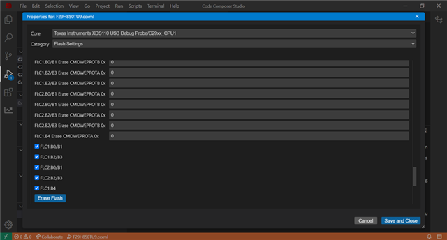
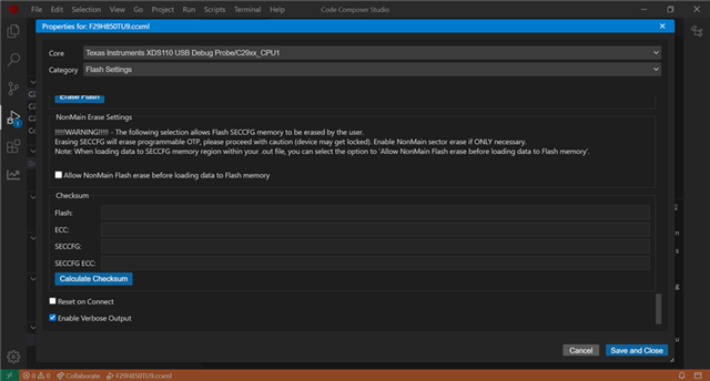
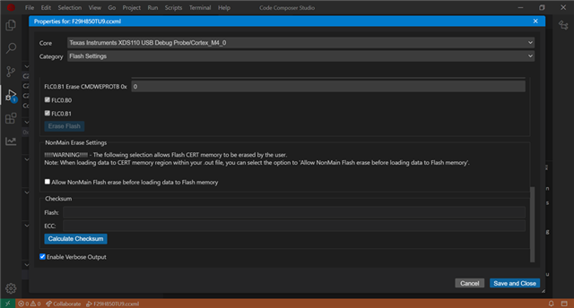
Question: How can I load a program that contains SECCFG memory regions?
Answer: The checkbox ‘Allow NonMain Flash erase before loading data to Flash memory’ must be selected if loading a program that wishes to change SECCFG memory region.
Question: How can I view the M4 Core Flash Settings?
Answer: M4 Flash Settings can be viewed by selecting the ‘Cortex_M4’ core selection and ‘Flash Settings’ category from the CPU Properties dialog box. Note that the M4 core does not have a Bank Mode selection compared to C29x CPU cores.
Question: How can I load a single-core example?
Answer:

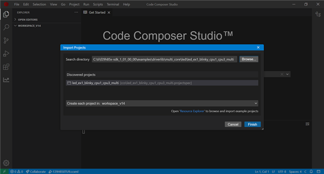
- To import a project, go to the File->Import Project(s) dropdown from the CCS taskbar
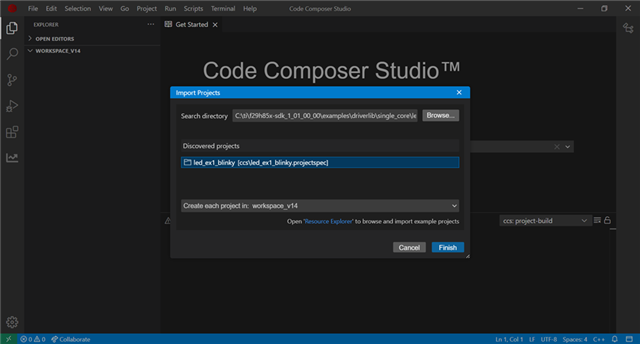
- The Import Projects dialog box will open, where you can then click on the browse button and navigate to the project in your F29 SDK for import
- This walkthrough uses the LED Blinky example for demonstration purposes
- Once the project is imported, its default Build Configuration will be RAM
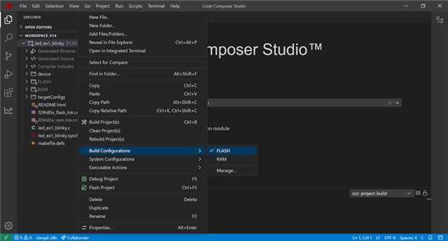
- To convert the Build Configuration to FLASH, right-click on the project, go to the Build Configuration dropdown and select FLASH
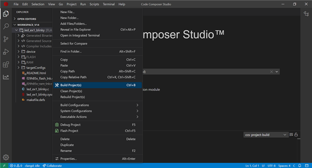
- Build the project with FLASH Build Configuration
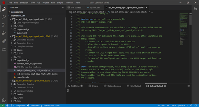
- Once the project has been built, a .out file will be generated within the project’s FLASH folder
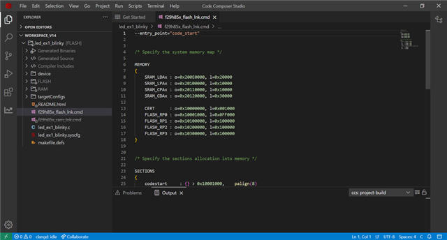
- To ensure the project is for the correct Build Configuration, you can also refer to the memory allocation of the flash linker command file used
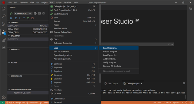
- From the Run taskbar, Select the Load->Load Program… option from the dropdown to load the program
- Once the program has loaded to the device, it will halt within the Main c function
- To demonstrate the example, select the ‘Continue’ option in the Debug menu symbol
Question: How can I load a multi-core example?
Answer:
- For Multi-Core examples, the process is similar to Single-Core loading
- From the Import Projects dialog box, click on the ‘Browse’ button and navigate to the project in your F29 SDK for import
- This demonstrate uses the Multi LED Blinky example
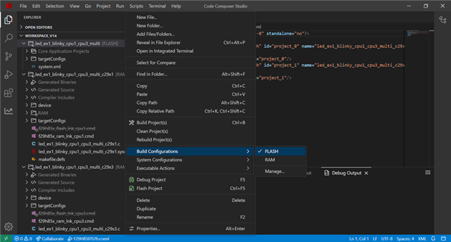
- Once the Multi-Core example has loaded, the default Build Configuration will be RAM
- Right-click on the project, go to the Build Configuration dropdown option and select FLASH
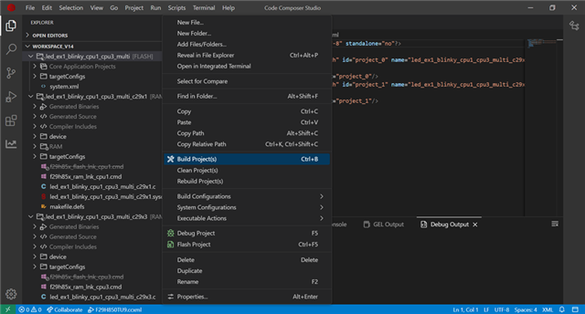
- Select the Build Project(s) option to build the Multi-Core Project
- Prior to loading the CPU core with the example, the Bank Mode needs to be set appropriately
- Set the BANK MODE to 2 and press the Program BANKMGMT button
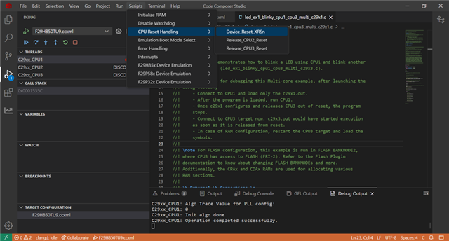
- After programming the BANK MODE to a mode with Multi-Core support for addressing, reset the device through either Device_Reset_XRSn/Power-On Reset
- Connect back to the target and proceed to load the CPU cores
- The Debug Output will show the current BANK MODE value for the device (BANK MODE 2 seen as 0x9)
- BANK MODE value can also be seen through the Device Register
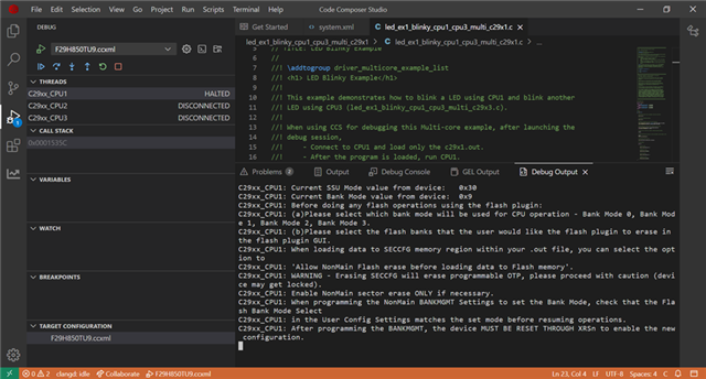
- Example instructions will be present in CPU1 as comments in the main .c file
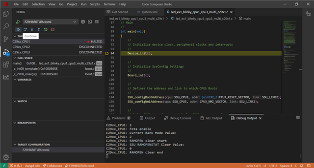
- Load CPU1 with the CPU1 .out file, CPU1 example will come to a halt within the Main function
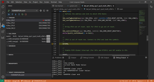
- Run CPU1 (CPU3 will release from reset)
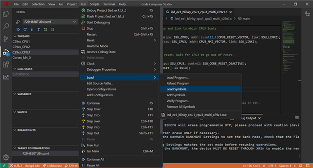
- Connect to CPU3, load the symbols for the project to CPU3’s core
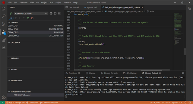
- Press ‘Continue’ for CPU1 core and ‘Continue’ for CPU3 core
- The Multi-Core LED Blinky example should now be running on the device
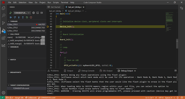
TMS320F29H85x Flash plugin usage notes:
(1) Before doing any flash operations using the flash plugin,
(a) Please select which bank mode will be used for CPU operation – Bank Mode 0, Bank Mode 1, Bank Mode 2, Bank Mode 3 (Note: This selection should be done in CPU1 flash plugin GUI).
(b) Please select the flash banks that the user would like the flash plugin to erase.
(2) When loading data to SECCFG memory region within your .out file, select the option to ‘Allow NonMain Flash erase before loading data to Flash memory’. Note - For verify failure when programming SECCFG memory region, unselect the ‘Verify flash program’ checkbox in the Flash Settings -> Download Settings box. An update will be provided in later release.
(3) The Flash Bank Mode Select in the User Config Settings will remember the previous bank mode the device is in. The actual bank mode can be determined by looking at the SSUGENREGS.BANKMODE register. After programming the desired Bank Mode, the device MUST BE RESET THROUGH XRSn to enable the new configuration.
(4) When loading data to the NonMain BANKMGMT and CERT memory regions within your .out file, select the option to ‘Allow NonMain Flash erase before loading data to Flash memory’. WARNING – Erasing NonMain BANKMGMT and CERT memory regions will erase programmable OTP, please proceed with caution. Enable NonMain sector erase ONLY if BANKMGMT or CERT programming is necessary.
Reference material:
F29H85x Real-Time Microcontrollers Data Manual
F29H85x Real-Time Microcontrollers Technical Reference Manual