This thread has been locked.
If you have a related question, please click the "Ask a related question" button in the top right corner. The newly created question will be automatically linked to this question.
Tool/software:
Hello,
I develop PSFB DCDC converter.
I use reference design TIDM-02000 and use TMS320F280039 MCU.
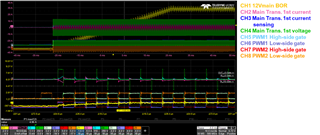
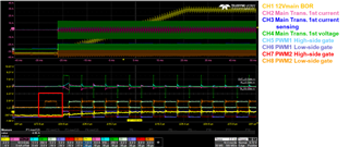
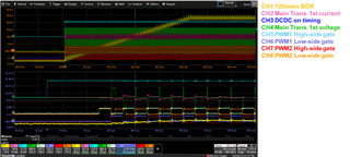
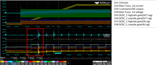
When DCDC turn on, Main Trans. 1st current peak current occured.
The I command value calculated by the MCU does not change and maintains a value close to 0.
The Main trans. 1st current increases, but the PWM gate does not turn off and remains on.
I wonder why. If there is anything to check, please let me know.
Thanks,
Best Regards,
Sangmo KIM.
Hi,
Our expert is out of office until the end of next week, please expect a delayed response.
Best Regards,
Ben Collier
Hi,
Thank for your reply.
There is costomer issus. So this is urgent issue.
Is there any other way to get support quickly?
Best Regards,
Sangmi KIM.
Sangmo,
In PSFB TIDM-02000, inner current loop is hardware based (comparator based peak current mode control). Initially, PWM of leading leg is 180deg phase shifted to lagging leg (same as shown in scope waveform you have shared). In this case, there is no power transfer. When sensed current is different than commanded current then phase is shift is adjusted using ePWM's cycle-by-cycle trips to adjust current flow in primary so that error can be mitigated. This type of trip resets at every switching cycle.
I would like to suggest couple of steps for debug,
1. Could you please cross-check current sensing circuitry to make sure that current signal is properly scaled and going to CMP/ADC input? You can remove shunt and use DC source or function generator to test this.
2. Internal comparator trip is connected to ePWM trip input?
3. Please make sure load is set to at least 25% of full load higher load so that current signal can be sensed properly.
4. Make sure blanking window is set to appropriate value so that there is no false cycle-by-cycle trip because switching transient.
Let me know if any of these remedies works.
Regards,
Sumit
Hi Sumit.
1. And I checked current sensing signal. This is normal. Please check below CH2 and CH3.
2. Yes, I know that Internal comparator trip is connected to ePWM trip input.
Please check code.
void PSFB_HAL_initCmpssPCMC(void)
{
//
// Enable CMPSS and configure the negative input signal to come from
// the DAC
//
CMPSS_enableModule(PSFB_PCMC_OCP_CMPSS_BASE); // CMPSS1 enable
CMPSS_configHighComparator(PSFB_PCMC_OCP_CMPSS_BASE, // High comparator (PCMC)
CMPSS_INSRC_DAC); // DAC Value : internal DAC
//
// Use DACL for OCP and configure the negative input signal to come from
// the DAC
//
CMPSS_configLowComparator(PSFB_PCMC_OCP_CMPSS_BASE, // CMPSS Low comparator (OCP)
CMPSS_INSRC_DAC); // DAC Value : internal DAC
//
// On 28004x, there is an additional MUX on the CMPSS,
// configured in the analogsysctrl
// Select positive input of CMPSSH to come from A2/B6/PGA1_OF (IHV_FB)
// Select positive input of CMPSSL to come from A2/B6/PGA1_OF (IHV_FB)
//
ASysCtl_selectCMPHPMux(PSFB_PCMC_OCP_CMPSS_ASYSCTRL_CMPHPMUX, // HP :High positive, LP : Low positive
PSFB_PCMC_OCP_CMPSS_ASYSCTRL_MUX_VALUE); // asys output?
ASysCtl_selectCMPLPMux(PSFB_PCMC_OCP_CMPSS_ASYSCTRL_CMPLPMUX,
PSFB_PCMC_OCP_CMPSS_ASYSCTRL_MUX_VALUE);
//
// Use VDDA as the reference for the DAC and set DAC value to
//
CMPSS_configDAC(PSFB_PCMC_OCP_CMPSS_BASE, CMPSS_DACREF_VDDA | // DAC Value -> Cmpss negative input
CMPSS_DACVAL_PWMSYNC | CMPSS_DACSRC_RAMP);
EALLOW;
//
// Set PWMSYNC as coming from ADC_OVERSAMPLE_PWM_BASE
//
HWREGH(PSFB_PCMC_OCP_CMPSS_BASE + CMPSS_O_COMPDACCTL) =
(HWREGH(PSFB_PCMC_OCP_CMPSS_BASE + CMPSS_O_COMPDACCTL) &
~(CMPSS_COMPDACCTL_RAMPSOURCE_M)) | (8);// 230227 8=>ePWM5, 4: ePWM3
EDIS;
CMPSS_setRampDecValue(PSFB_PCMC_OCP_CMPSS_BASE, PSFB_SLOPE_INITIAL);
//
// DAC Initialization
//
CMPSS_setMaxRampValue(PSFB_PCMC_OCP_CMPSS_BASE, PSFB_PCMC_DAC_INIT);
CMPSS_setDACValueLow(PSFB_PCMC_OCP_CMPSS_BASE, PSFB_OCP_DAC_INIT); // Low Cmpss : IHV_FB OCP intial Setting. 3584/4096
CMPSS_configFilterLow(PSFB_PCMC_OCP_CMPSS_BASE, PSFB_OCP_SAMPLE_PRESCALE,
PSFB_OCP_SAMPLE_WINDOW, PSFB_OCP_THRESHOLD); // Digital filter 10 sample >= 7
CMPSS_configFilterHigh(PSFB_PCMC_OCP_CMPSS_BASE, 0,
4, 4); // Digital filter 10 sample >= 7
//
// Initialize digital filter
//
CMPSS_initFilterHigh(PSFB_PCMC_OCP_CMPSS_BASE);
CMPSS_initFilterLow(PSFB_PCMC_OCP_CMPSS_BASE);
//
// Configure the output signals. Both CTRIPH and CTRIPOUTH will be fed by
// the asynchronous comparator output.
//
// CMPSS_configOutputsHigh(PSFB_PCMC_OCP_CMPSS_BASE,
// CMPSS_TRIP_ASYNC_COMP | CMPSS_TRIPOUT_ASYNC_COMP);
CMPSS_configOutputsHigh(PSFB_PCMC_OCP_CMPSS_BASE,
CMPSS_TRIP_FILTER | CMPSS_TRIPOUT_FILTER);
CMPSS_configOutputsLow(PSFB_PCMC_OCP_CMPSS_BASE,
CMPSS_TRIP_FILTER | CMPSS_TRIPOUT_FILTER);
//
// Clear the latched comparator events
//
CMPSS_clearFilterLatchHigh(PSFB_PCMC_OCP_CMPSS_BASE);
CMPSS_clearFilterLatchLow(PSFB_PCMC_OCP_CMPSS_BASE);
}
3. I do not understand this comment.
You are meaning, If I want sensing 10A, I must set maximun curent scale 40A?
4. I use dcdc switching frequency 55kHz, And I set blanking windows 100ns.
Could you comment to me how i set blanking window to appropriate value?
I have other question.
I enable PWM function below chart.
If DCDC turn on, enable PWM port first, than PWM forcr trip clear.
On going PWM function enable, abnormal PWM output.
You can see red box blow waveform.
I want know why PWM2 Low-side gate output during PWM function enable.
Please check.
I can avoid abnormal PWM output during PWM funciotn enable to change sequence PWM funciotn enable.
thanks,
Sangmo Kim.
Sangmo,
There is similar e2e that discusses debug steps about the exact issue that you are facing. Could you please follow the same steps https://e2e.ti.com/support/microcontrollers/c2000-microcontrollers-group/c2000/f/c2000-microcontrollers-forum/1465785/tidm-02000-query-regarding-slope-compensation-in-3kw-dc-dc-converter-design-based-on-tidm-02000
Regards,
Sumit