This is related to the discussion here: question
and here:
[FAQ]
Following the solution from the FAQ sometimes works, but not always. It appears that something gets "stuck" after repeated flashing or debug sessions. It never works when you allow the GUI Composer to flash the device, and then the FAQ solution also stops working for some time.
Following the FAQ solution from a clean power-up:
- Start project-less debug from TMS320F28P650DK9.ccxml (created from example project)
- Connect to both cores
- Properties>CPU1>Flash settings > configure bank 0-2 for CPU1 and 3-4 for CPU2
- Erase settings: only erase bank 0-2
- Configure clock
- Save and close
- Continue CPU1
- Load>(my program, an example program, it doesn't seem to matter)
- Properties>CPU2> Note that the flash bank map settings are greyed out and all are set to 0
- Erase settings: only erase banks 3 and 4
- Save and close
- Continue CPU2
- Run>Load> my program
- Success

Try to open a GUI Composer program, and realize that it tried to flash the program again (despite `symbolsOnly=true` in the gc-model-program) and failed:
So we try the previous steps again
- Start debugging
- Connect both cores
- Check configuration is still good
- Configure clock
- Run, then load CPU1
- Check CPU2 configuartion
- Run, then load CPU2
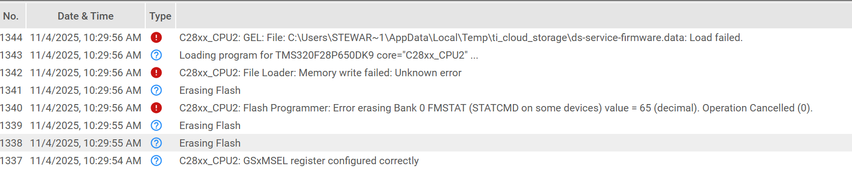
- Fail:
Power cycle, try again, it still fails. Eventually I can try to flash and reflash and get it to work, but it's about 1 in 10 attempts.
A couple of things I've noticed that could be clues:
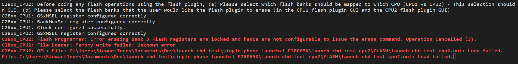
- When I flash CPU1, the popup in the bottom right corner will say something to the effect of "Erasing Bank 0", then "Erasing Bank 1", then 2 and then also 3 briefly before continuing on - despite bank 3 being configured for CPU2 and not checked to be erased with CPU1
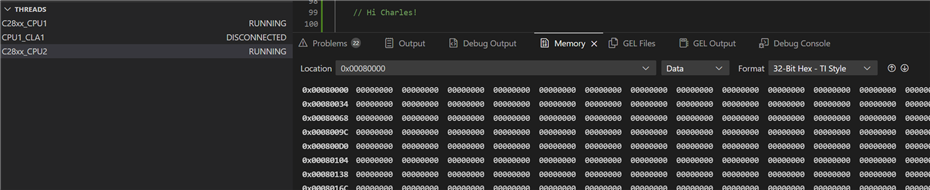
- If I do a "Blank Check" in the error state, this is the message: C28xx_CPU2: Flash Programmer: Error during Blank Check @ address 0x00080000; expected 0xFFFFFFFF, actual 0x00000000 (0).
Does that suggest that the "erase" function is filling with 0 instead of F? Is that a configuration option?