


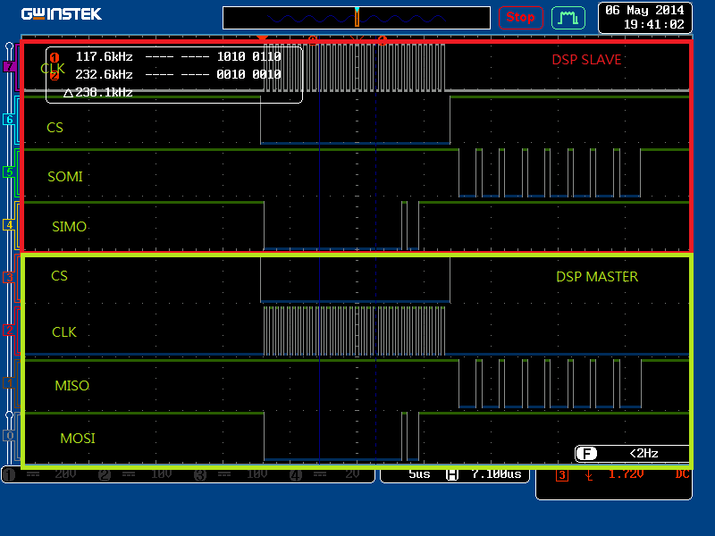
My Code:
//###########################################################################
//
// FILE:	Example_2833xMCBSP_SPIX.c
//
// TITLE:	DSP28133x Device McBSP using SPI mode
//
// ASSUMPTIONS:
//
//    This program requires the DSP2833x header files.
//    As supplied, this project is configured for "boot to SARAM"
//    operation.  The 2833x Boot Mode table is shown below.
//    For information on configuring the boot mode of an eZdsp,
//    please refer to the documentation included with the eZdsp,
//
//       $Boot_Table:
//
//         GPIO87   GPIO86     GPIO85   GPIO84
//          XA15     XA14       XA13     XA12
//           PU       PU         PU       PU
//        ==========================================
//            1        1          1        1    Jump to Flash
//            1        1          1        0    SCI-A boot
//            1        1          0        1    SPI-A boot
//            1        1          0        0    I2C-A boot
//            1        0          1        1    eCAN-A boot
//            1        0          1        0    McBSP-A boot
//            1        0          0        1    Jump to XINTF x16
//            1        0          0        0    Jump to XINTF x32
//            0        1          1        1    Jump to OTP
//            0        1          1        0    Parallel GPIO I/O boot
//            0        1          0        1    Parallel XINTF boot
//            0        1          0        0    Jump to SARAM	    <- "boot to SARAM"
//            0        0          1        1    Branch to check boot mode
//            0        0          1        0    Boot to flash, bypass ADC cal
//            0        0          0        1    Boot to SARAM, bypass ADC cal
//            0        0          0        0    Boot to SCI-A, bypass ADC cal
//                                              Boot_Table_End$
//
// DESCRIPTION:
//
// SPI master mode transfer of 32-bit word size with digital loopback enabled.
//
//           McBSP Signals      SPI equivalent
//           -------------------------------------
//           MCLKX              SPICLK  (master)
//           MFSX               SPISTE  (master)
//           MDX                SPISIMO
//           MCLKR              SPICLK  (slave - not used for this example)
//           MFSR               SPISTE  (slave - not used for this example)
//           MDR                SPISOMI (not used for this example)
//
// This program will execute and transmit words until terminated by the user.
//
// By default for the McBSP examples, the McBSP sample rate generator (SRG) input
// clock frequency is LSPCLK (150E6/4 or 100E6/4) assuming SYSCLKOUT = 150 MHz or
// 100 MHz respectively.  If while testing, the SRG input frequency
// is changed, the #define MCBSP_SRG_FREQ  (CPU_SPD/4) in the Mcbsp.c file must
// also be updated accordingly.  This define is used to determine the Mcbsp initialization
// delay after the SRG is enabled, which must be at least 2 SRG clock cycles.
//
//          Watch Variables:
//                sdata1
//                sdata2
//                rdata1
//                rdata2
//
//
//###########################################################################
//
// Original Author: S.S.
//
// $TI Release: 2833x/2823x Header Files and Peripheral Examples V133 $
// $Release Date: June 8, 2012 $
//###########################################################################

#include "DSP28x_Project.h"     // Device Headerfile and Examples Include File

#define _EN_SLAVE 	0

interrupt void cpu_timer0_isr(void);
interrupt void cpu_timer1_isr(void);
interrupt void cpu_timer2_isr(void);

interrupt void mcbsp_spiTxIsr(void);
interrupt void mcbsp_spiRxIsr(void);
// Prototype statements for functions found within this file.

void init_mcbsp_spi(void);
void mcbsp_xmit(int32 data);
void error(void);

// Global data for this example
int32 sdata = 0;    // Sent Data
int32 rdata = 0;    // Recieved Data


void main(void)
{

//   Uint16 i;


// Step 1. Initialize System Control:
// PLL, WatchDog, enable Peripheral Clocks
// This example function is found in the DSP2833x_SysCtrl.c file.
   InitSysCtrl();

// Step 2. Initalize GPIO:
// This example function is found in the DSP2833x_Gpio.c file and
// illustrates how to set the GPIO to it's default state.
// InitGpio();  // Skipped for this example
// For this example, only enable the GPIO for McBSP-A
   InitMcbspaGpio();

// Step 3. Clear all interrupts and initialize PIE vector table:
// Disable CPU interrupts
   DINT;

// Initialize PIE control registers to their default state.
// The default state is all PIE interrupts disabled and flags
// are cleared.
// This function is found in the DSP2833x_PieCtrl.c file.
   InitPieCtrl();

// Disable CPU interrupts and clear all CPU interrupt flags:
   IER = 0x0000;
   IFR = 0x0000;

// Initialize the PIE vector table with pointers to the shell Interrupt
// Service Routines (ISR).
// This will populate the entire table, even if the interrupt
// is not used in this example.  This is useful for debug purposes.
// The shell ISR routines are found in DSP281x_DefaultIsr.c.
// This function is found in DSP2833x_PieVect.c.
   InitPieVectTable();

// Interrupts that are used in this example are re-mapped to
// ISR functions found within this file.
	EALLOW;	// This is needed to write to EALLOW protected registers
	PieVectTable.TINT0 = &cpu_timer0_isr;
	PieVectTable.XINT13 = &cpu_timer1_isr;
	PieVectTable.TINT2 = &cpu_timer2_isr;
	PieVectTable.MRINTA = &mcbsp_spiRxIsr;
	PieVectTable.MXINTA = &mcbsp_spiTxIsr;
	EDIS;   // This is needed to disable write to EALLOW protected registers

// Step 4. Initialize all the Device Peripherals:
// This function is found in DSP2833x_InitPeripherals.c
// InitPeripherals();     // Not required for this example
    InitCpuTimers();   // For this example, only initialize the Cpu Timers

#if (CPU_FRQ_150MHZ)
// Configure CPU-Timer 0, 1, and 2 to interrupt every second:
// 150MHz CPU Freq, 1 second Period (in uSeconds)
	ConfigCpuTimer(&CpuTimer0, 150, 1000000);
	ConfigCpuTimer(&CpuTimer1, 150, 1000000);
	ConfigCpuTimer(&CpuTimer2, 150, 1000000);
#endif

// Step 5. User specific code,

	init_mcbsp_spi();


	CpuTimer0Regs.TCR.all = 0x4001; // Use write-only instruction to set TSS bit = 0
	CpuTimer1Regs.TCR.all = 0x4001; // Use write-only instruction to set TSS bit = 0
	CpuTimer2Regs.TCR.all = 0x4001; // Use write-only instruction to set TSS bit = 0

	// Enable interrupts required for this example
	PieCtrlRegs.PIECTRL.bit.ENPIE = 1;   // Enable the PIE block
	PieCtrlRegs.PIEIER6.bit.INTx1=1;     // Enable PIE Group 6, INT 1
	PieCtrlRegs.PIEIER6.bit.INTx2=1;     // Enable PIE Group 6, INT 2
	PieCtrlRegs.PIEIER6.bit.INTx5=1;     // Enable PIE Group 6, INT 5
	PieCtrlRegs.PIEIER6.bit.INTx6=1;     // Enable PIE Group 6, INT 6
	// Enable TINT0 in the PIE: Group 1 interrupt 7
	PieCtrlRegs.PIEIER1.bit.INTx7 = 1;
	IER=M_INT6|M_INT1|M_INT13|M_INT14;     // Enable CPU INT6

	EINT;   // Enable Global interrupt INTM
	ERTM;   // Enable Global realtime interrupt DBGM

	// Step 6. IDLE loop. Just sit and loop forever (optional):
	for(;;);

}


// Some Useful local functions

void error(void)
{
    asm("     ESTOP0");  // test failed!! Stop!
    for (;;);
}


void init_mcbsp_spi()
{
	// McBSP-A register settings
	McbspaRegs.SPCR2.all=0x0000; 		// Reset FS generator, sample rate generator & transmitter
	McbspaRegs.SPCR1.all=0x0000; 		// Reset Receiver, Right justify word, Digital loopback dis.
#if _EN_SLAVE
	McbspaRegs.PCR.all=0x0008; 			//(CLKXM=CLKRM=FSXM=FSRM= 0, FSXP = 1)
	McbspaRegs.SPCR1.bit.CLKSTP = 2; 	// Together with CLKXP/CLKRP determines clocking scheme
	McbspaRegs.PCR.bit.CLKXP = 0; 		// CPOL = 0, CPHA = 0 rising edge no delay
	McbspaRegs.PCR.bit.CLKRP = 0;
	McbspaRegs.RCR2.bit.RDATDLY=00; 	// FSX setup time 1 in master mode. 0 for slave mode (Receive)
	McbspaRegs.XCR2.bit.XDATDLY=00; 	// FSX setup time 1 in master mode. 0 for slave mode (Transmit)
	McbspaRegs.RCR1.bit.RWDLEN1=5;     	// 32-bit word
	McbspaRegs.XCR1.bit.XWDLEN1=5;     	// 32-bit word

#else
	McbspaRegs.PCR.all=0x0F08;           //(CLKXM=CLKRM=FSXM=FSRM= 1, FSXP = 1)
	McbspaRegs.SPCR1.bit.DLB = 0;		 // LoopBack Mode Enable/Disable
	McbspaRegs.SPCR1.bit.CLKSTP = 2;     // Together with CLKXP/CLKRP determines clocking scheme
	McbspaRegs.PCR.bit.CLKXP = 0;		 // CPOL = 0, CPHA = 0 rising edge no delay
	McbspaRegs.PCR.bit.CLKRP = 0;
	McbspaRegs.RCR2.bit.RDATDLY=01;      // FSX setup time 1 in master mode. (Receive)
	McbspaRegs.XCR2.bit.XDATDLY=01;      // FSX setup time 1 in master mode. (Transmit)
	McbspaRegs.RCR1.bit.RWDLEN1=5;     	// 32-bit word
	McbspaRegs.XCR1.bit.XWDLEN1=5;     	// 32-bit word
#endif


	//McbspaRegs.MFFINT.bit.XINT = 1; 	// Enable Transmit Interrupts
	//McbspaRegs.MFFINT.bit.RINT = 1; 	// Enable Receive Interrupts

	McbspaRegs.SRGR2.all=0x2000; 	 	 // CLKSM=1, FPER = 1 CLKG periods
	McbspaRegs.SRGR1.all= 0x000F;	     // Frame Width = 1 CLKG period, CLKGDV=1~255

	McbspaRegs.SPCR2.bit.GRST=1;         // Enable the sample rate generator
	delay_loop();                        // Wait at least 2 SRG clock cycles
	McbspaRegs.SPCR2.bit.XRST=1;         // Release TX from Reset
	McbspaRegs.SPCR1.bit.RRST=1;         // Release RX from Reset
	McbspaRegs.SPCR1.bit.RINTM = 1;         // Release RX from Reset
	McbspaRegs.SPCR2.bit.FRST=1;         // Frame Sync Generator reset
}


void mcbsp_xmit(int32 data)
{
    McbspaRegs.DXR2.all=data>>16;
    McbspaRegs.DXR1.all=data;
}


interrupt void mcbsp_spiTxIsr(void)
{

    // To receive more interrupts from this PIE group, acknowledge this interrupt
    PieCtrlRegs.PIEACK.all = PIEACK_GROUP6;
}

interrupt void mcbsp_spiRxIsr(void)
{

#if _EN_SLAVE
	long rdata = 0;
    rdata=McbspaRegs.DRR2.all;
    rdata<<=16;
    rdata|=McbspaRegs.DRR1.all;

    // To receive more interrupts from this PIE group, acknowledge this interrupt
    PieCtrlRegs.PIEACK.all = PIEACK_GROUP6;
#else
	long rdata = 0;
    rdata=McbspaRegs.DRR1.all;
    rdata<<=16;
    rdata|=McbspaRegs.DRR2.all;
    // To receive more interrupts from this PIE group, acknowledge this interrupt
    PieCtrlRegs.PIEACK.all = PIEACK_GROUP6;
#endif

}

interrupt void cpu_timer0_isr(void)
{
	CpuTimer0.InterruptCount++;
#if _EN_SLAVE
	mcbsp_xmit(0x88888888);
#else
	sdata = (sdata + 1)%360;
	mcbsp_xmit(sdata);
#endif
	// Acknowledge this interrupt to receive more interrupts from group 1
	PieCtrlRegs.PIEACK.all = PIEACK_GROUP1;
}

interrupt void cpu_timer1_isr(void)
{
   CpuTimer1.InterruptCount++;
   // The CPU acknowledges the interrupt.
   EDIS;
}

interrupt void cpu_timer2_isr(void)
{  EALLOW;
   CpuTimer2.InterruptCount++;
   // The CPU acknowledges the interrupt.
   EDIS;
}


//===========================================================================
// No more.
//===========================================================================
I tried to use McBsp's interrupt in SPI Mode, then communicate between both.
But I can send a 32bits data out from Master, but I can not receive any data from Slave.
Who can help me to solve it?
Thank you first.

