


Dear All,
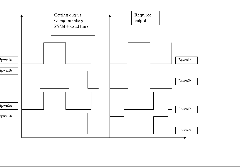
I use the ePWM module from F28069 and i have to generate the two sets of complimentary PWM signal with dead band (EPWM1A, EPWM1B & EPWM2A, EPWM2B).
But i want
EPWM1A, EPWM2B signals start at same time(synchronous) , EPWM1A, EPWM1B signals complimentary with dead band.
EPWM1B,EPWM2A at same time synchronous),EPWM2A, EPWM2B signals complimentary with dead band.
Because to drive H BRIGE converter
EPWM1A,EPWM1B signals are connected in series of switches s23 and s73 in left side leg of Hbridge inverter
EPWM2A,EPWM2B are connected in series of switches s24 and s74 in Right side leg of Hbridge inverter
for one cycle EPWM1A and EPWM2B should ON
For other cycle EPWM2A and EPWM1B should ON
I configured the both PWMx as active high complimentary and configured the deadband full enable. But i did not get the proper output.
This is the PWM configuration source code
#include "PeripheralHeaderIncludes.h"
#include "F2806x_EPwm_defines.h" // useful defines for initialization
//%%%%%%%%%%%%%%%%%%%%%%%%%%%%%%%%%%%%%%%%%%%%%%%%%%%%%%%%%%%%%%%%%%%%%%%%%%%%%%%%%%
// FUNCTION PROTOTYPES
//%%%%%%%%%%%%%%%%%%%%%%%%%%%%%%%%%%%%%%%%%%%%%%%%%%%%%%%%%%%%%%%%%%%%%%%%%%%%%%%%%%
void DeviceInit(void);
void InitFlash(void);
void MemCopy(Uint16 *SourceAddr, Uint16* SourceEndAddr, Uint16* DestAddr);
//%%%%%%%%%%%%%%%%%%%%%%%%%%%%%%%%%%%%%%%%%%%%%%%%%%%%%%%%%%%%%%%%%%%%%%%%%%%%%%%%%%
// VARIABLE DECLARATIONS - GENERAL
//%%%%%%%%%%%%%%%%%%%%%%%%%%%%%%%%%%%%%%%%%%%%%%%%%%%%%%%%%%%%%%%%%%%%%%%%%%%%%%%%%%
// Used for running BackGround in flash and the ISR in RAM
extern Uint16 RamfuncsLoadStart, RamfuncsLoadEnd, RamfuncsRunStart;
//Uint16 RED_delay=30; // 375ns when PLL is set to 0x10 (80MHz)
//Uint16 FED_delay=30; // 375ns when PLL is set to 0x10 (80MHz)
//Uint16 RED_delay=80; // 375ns when PLL is set to 0x10 (80MHz)
//Uint16 FED_delay=80; // 375ns when PLL is set to 0x10 (80MHz)
Uint16 RED_delay=80; // 375ns when PLL is set to 0x10 (80MHz)
Uint16 FED_delay=80; // 375ns when PLL is set to 0x10 (80MHz)
//%%%%%%%%%%%%%%%%%%%%%%%%%%%%%%%%%%%%%%%%%%%%%%%%%%%%%%%%%%%%%%%%%%%%%%%%%%%%%%%%%%
// MAIN CODE - starts here
//%%%%%%%%%%%%%%%%%%%%%%%%%%%%%%%%%%%%%%%%%%%%%%%%%%%%%%%%%%%%%%%%%%%%%%%%%%%%%%%%%%
void main(void)
{
//=================================
// INITIALISATION - General
//=================================
DeviceInit(); // Device Life support & GPIO mux settings
// Only used if running from FLASH
// Note that the variable FLASH is defined by the compiler (-d FLASH)
#ifdef FLASH
// Copy time critical code and Flash setup code to RAM
// The RamfuncsLoadStart, RamfuncsLoadEnd, and RamfuncsRunStart
// symbols are created by the linker. Refer to the linker files.
MemCopy(&RamfuncsLoadStart, &RamfuncsLoadEnd, &RamfuncsRunStart);
// Call Flash Initialization to setup flash waitstates
// This function must reside in RAM
InitFlash(); // Call the flash wrapper init function
#endif //(FLASH)
//-------------------------------------------------------------
//#define period 1000 // 80kHz when PLL is set to 0x10 (80MHz)
//#define period 500 // 160kHz when PLL is set to 0x10 (80MHz)
#define period 1600 //50khz
// Time-base registers
EPwm1Regs.TBPRD = period; // Set timer period, PWM frequency = 1 / period
EPwm2Regs.TBPRD = period; // Set timer period, PWM frequency = 1 / period
EPwm1Regs.TBPHS.all = 0; // Time-Base Phase Register
EPwm2Regs.TBPHS.all = 0; // Time-Base Phase Register
EPwm1Regs.TBCTR = 0; // Time-Base Counter Register
EPwm2Regs.TBCTR = 0; // Time-Base Counter Register
EPwm1Regs.TBCTL.bit.PRDLD = TB_IMMEDIATE; // Set Immediate load
EPwm2Regs.TBCTL.bit.PRDLD = TB_IMMEDIATE; // Set Immediate load
EPwm1Regs.TBCTL.bit.CTRMODE = TB_COUNT_UP; // Count-up mode: used for asymmetric PWM
EPwm2Regs.TBCTL.bit.CTRMODE = TB_COUNT_UP; // Count-up mode: used for asymmetric PWM
EPwm1Regs.TBCTL.bit.PHSEN = TB_DISABLE; // Disable phase loading
EPwm2Regs.TBCTL.bit.PHSEN = TB_DISABLE; // Disable phase loading
EPwm1Regs.TBCTL.bit.SYNCOSEL = TB_SYNC_DISABLE;
EPwm2Regs.TBCTL.bit.SYNCOSEL = TB_SYNC_DISABLE;
EPwm1Regs.TBCTL.bit.HSPCLKDIV = TB_DIV1;
EPwm2Regs.TBCTL.bit.HSPCLKDIV = TB_DIV1;
EPwm1Regs.TBCTL.bit.CLKDIV = TB_DIV1;
EPwm2Regs.TBCTL.bit.CLKDIV = TB_DIV1;
// Setup shadow register load on ZERO
EPwm1Regs.CMPCTL.bit.SHDWAMODE = CC_SHADOW;
EPwm2Regs.CMPCTL.bit.SHDWAMODE = CC_SHADOW;
EPwm1Regs.CMPCTL.bit.SHDWBMODE = CC_SHADOW;
EPwm2Regs.CMPCTL.bit.SHDWBMODE = CC_SHADOW;
EPwm1Regs.CMPCTL.bit.LOADAMODE = CC_CTR_ZERO; // load on CTR=Zero
EPwm2Regs.CMPCTL.bit.LOADAMODE = CC_CTR_ZERO; // load on CTR=Zero
EPwm1Regs.CMPCTL.bit.LOADBMODE = CC_CTR_ZERO; // load on CTR=Zero
EPwm2Regs.CMPCTL.bit.LOADBMODE = CC_CTR_ZERO; // load on CTR=Zero
// Set actions
EPwm1Regs.AQCTLA.bit.ZRO = AQ_SET; // Set PWM2A on Zero
EPwm2Regs.AQCTLA.bit.ZRO = AQ_SET; // Set PWM2A on Zero
EPwm1Regs.AQCTLA.bit.CAU = AQ_CLEAR; // Clear PWM2A on event A, up count
EPwm2Regs.AQCTLA.bit.CAU = AQ_CLEAR; // Clear PWM2A on event A, up count
EPwm1Regs.AQCTLB.bit.ZRO = AQ_CLEAR; // Set PWM2B on Zero
EPwm2Regs.AQCTLB.bit.ZRO = AQ_CLEAR; // Set PWM2B on Zero
EPwm1Regs.AQCTLB.bit.CBU = AQ_SET; // Clear PWM2B on event B, up count
EPwm2Regs.AQCTLB.bit.CBU = AQ_SET; // Clear PWM2B on event B, up count
// DeadBand configuration
EPwm1Regs.DBCTL.bit.IN_MODE = DBA_ALL; // EPWM2A is the source for both falling-edge and rising-edge delay
EPwm2Regs.DBCTL.bit.IN_MODE = DBA_ALL; // EPWM2A is the source for both falling-edge and rising-edge delay
EPwm1Regs.DBCTL.bit.OUT_MODE = DB_FULL_ENABLE;
EPwm2Regs.DBCTL.bit.OUT_MODE = DB_FULL_ENABLE; // Both the falling-edge delay (FED) and rising-edge delay (RED) are applied to the input signals
EPwm1Regs.DBCTL.bit.POLSEL = DB_ACTV_HIC;
EPwm2Regs.DBCTL.bit.POLSEL = DB_ACTV_HIC; // Active High Complementary (AHC)
EPwm1Regs.CMPA.half.CMPA = period/2; // Set duty 50% initially
EPwm2Regs.CMPA.half.CMPA = period/2; // Set duty 50% initially
EPwm1Regs.CMPB = period/2; // Set duty 50% initially
EPwm2Regs.CMPB = period/2; // Set duty 50% initially
EPwm1Regs.DBRED = RED_delay;
EPwm2Regs.DBRED = RED_delay; // Set DeadBand time for rising edge
EPwm1Regs.DBFED = FED_delay;
EPwm2Regs.DBFED = FED_delay; // Set DeadBand time for falling edge
// For further details see Fig2-28 in SPRU791.PDF (TMS320x28xx,
// Enhanced Pulse Width Modulator Module)
/*EPwm1Regs.TBPRD = 800; // Period = 2´600 TBCLK counts
EPwm2Regs.TBPRD = 800; // Period = 2´600 TBCLK counts
EPwm1Regs.CMPA.half.CMPA = 400; // Compare A = 350 TBCLK counts
EPwm2Regs.CMPA.half.CMPA = 400; // Compare A = 350 TBCLK counts
EPwm1Regs.CMPB = 320; // Compare B = 400 TBCLK counts
EPwm2Regs.CMPB = 320; // Compare B = 400 TBCLK counts
EPwm1Regs.TBPHS.all = 0; // Set Phase register to zero
EPwm2Regs.TBPHS.all = 0; // Set Phase register to zero
EPwm1Regs.TBCTR = 0; // clear TB counter
EPwm2Regs.TBCTR = 0; // clear TB counter
EPwm1Regs.TBCTL.bit.CTRMODE = TB_COUNT_UPDOWN; // Symmetric
EPwm2Regs.TBCTL.bit.CTRMODE = TB_COUNT_UPDOWN; // Symmetric
EPwm1Regs.TBCTL.bit.PHSEN = TB_DISABLE; // Phase loading disabled
EPwm2Regs.TBCTL.bit.PHSEN = TB_DISABLE; // Phase loading disabled
EPwm1Regs.TBCTL.bit.PRDLD = TB_IMMEDIATE;
EPwm2Regs.TBCTL.bit.PRDLD = TB_IMMEDIATE;
EPwm1Regs.TBCTL.bit.SYNCOSEL = TB_SYNC_DISABLE;
EPwm2Regs.TBCTL.bit.SYNCOSEL = TB_SYNC_DISABLE;
EPwm1Regs.TBCTL.bit.HSPCLKDIV = TB_DIV1; // TBCLK = SYSCLKOUT
EPwm2Regs.TBCTL.bit.HSPCLKDIV = TB_DIV1; // TBCLK = SYSCLKOUT
EPwm1Regs.TBCTL.bit.CLKDIV = TB_DIV1;
EPwm2Regs.TBCTL.bit.CLKDIV = TB_DIV1;
EPwm1Regs.CMPCTL.bit.SHDWAMODE = CC_IMMEDIATE;
EPwm2Regs.CMPCTL.bit.SHDWAMODE = CC_IMMEDIATE;
EPwm1Regs.CMPCTL.bit.SHDWBMODE = CC_IMMEDIATE;
EPwm2Regs.CMPCTL.bit.SHDWBMODE = CC_IMMEDIATE;
EPwm1Regs.CMPCTL.bit.LOADAMODE = CC_CTR_ZERO; // load on CTR = Zero
EPwm2Regs.CMPCTL.bit.LOADAMODE = CC_CTR_ZERO; // load on CTR = Zero
EPwm1Regs.CMPCTL.bit.LOADBMODE = CC_CTR_ZERO; // load on CTR = Zero
EPwm2Regs.CMPCTL.bit.LOADBMODE = CC_CTR_ZERO; // load on CTR = Zero
EPwm1Regs.AQCTLA.bit.CAU = AQ_SET;
EPwm2Regs.AQCTLA.bit.CAU = AQ_CLEAR;
EPwm1Regs.AQCTLA.bit.CAD = AQ_CLEAR;
EPwm2Regs.AQCTLA.bit.CAD = AQ_SET;
EPwm1Regs.AQCTLB.bit.CBU = AQ_CLEAR;
EPwm2Regs.AQCTLB.bit.CBU = AQ_SET;
EPwm1Regs.AQCTLB.bit.CBD = AQ_SET;
EPwm2Regs.AQCTLB.bit.CBD = AQ_CLEAR;*/
for(;;)
{
}
}
Please give valid suggestion to solve the problem
Thanks & Regards,
Muthu

