This thread has been locked.

If you have a related question, please click the "Ask a related question" button in the top right corner. The newly created question will be automatically linked to this question.

TMS320F28335: Internal A/D Behavior

Part Number: TMS320F28335
Other Parts Discussed in Thread: TMS320F28035

Hello there,

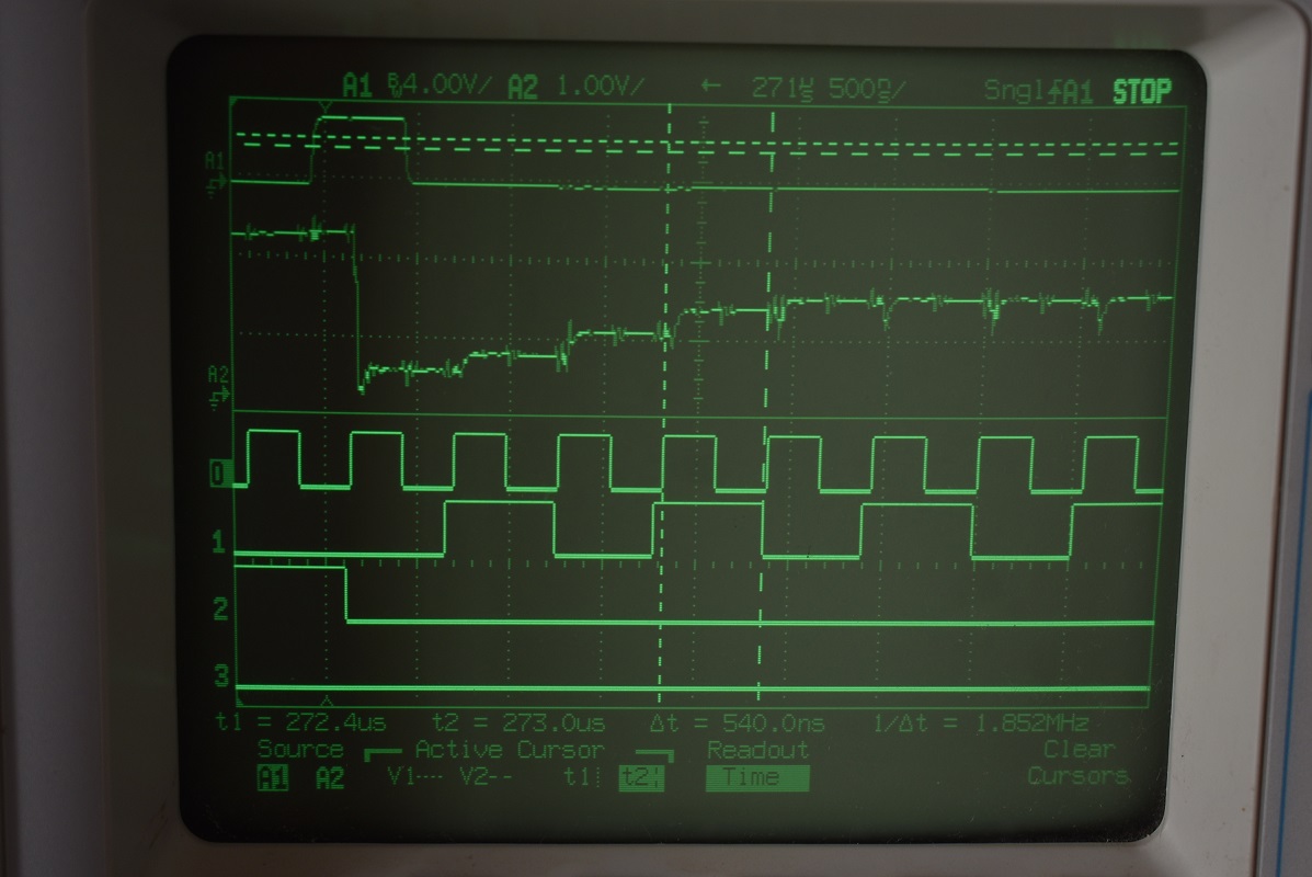
I have a customer using this device who has been witnessing interesting behavior. What he is seeing is very similar to what is described in the attached from the device's errata but his set-up is a bit different.

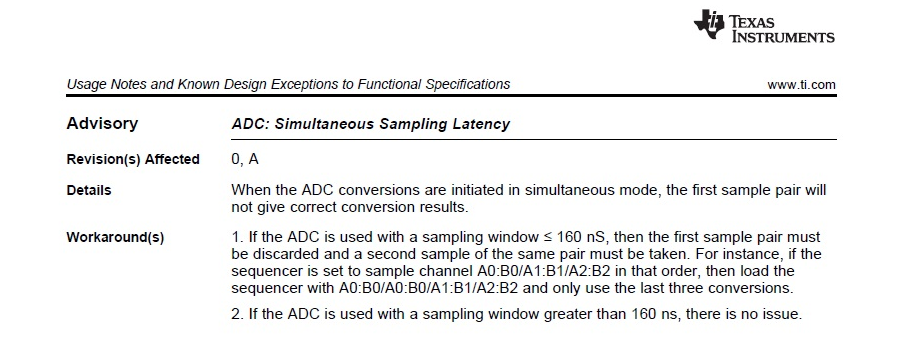
The difference is, that he is using the A/D in sequential mode rather than simultaneous. He is finding that at times, the first reading is not accurate – always overstated, often times FFFh.  And, if their test method is valid, when an incorrect reading is given, the A/D takes measurably less time to set the busy flag after SOC than when a correct reading is given.


The CPU is at 150mHz and the A/D is at 25mHz with a sample window of 1 (low impedance source).  It happens when SOC’d by the EPWM module and by software trigger.  He is using the internal reference.  It is being supplied at 1.9V / 3.3V.  They understand they're pushing the processor to it's limit but historically doing so has given them good results.


The customer is currently using the workaround suggested – just taking an initial conversion and discarding – but he also wants to gain some assurance that there isn’t something else wrong since the operational conditions do not exactly match that given on the errata.


Appreciate any feedback you can provide on this!

-Amanda

  • Amanda,

    I am not aware of any issues like this that are not already described in the errata document. In this case, I don't know what assurances we can provide without understanding what is going wrong in their system.

    I assume that this is for a custom board vs a TI EVM. Is the behavior observed on multiple devices? Did this configuration work in the past, but recently started having trouble? Is it a new design based on an old system?

    -Tommy
  • Hello Tlee,

    Thank you for your quick response. The behavior is occurring on a custom board and it has happened on three so far while my customer has been testing. Historically in other versions of their product, the customer has used the ADC module within the TMS320F28035 but has not seen the same behavior.

    I have attached a scope shot describing what they're seeing.

    AD Issue.pdf

    The two observations in question are as follows--

    - Early completion and bad reading on the 1st 2 samples.

    - Slower than expected conversion cycle.

    Is this the norm in conjunction with the errata or have you witness this before as being attributed to something else possibly?

    Thank you for your time,

    -Amanda

  • Amanda,

    The wave forms do look strange. I would not expect the completion flag times to vary as shown.

    Would the customer be interested in letting us review the ADC code? The ADC architecture is notably different between F2803x and F2833x so there might be some small nuance that is contributing to this behavior.

    Is it possible that multiple SOC sources have been enabled for the sequencer? That might explain the early completion signal.

    -Tommy
  • Hello Tommy,

    The 1st sequencer is only used for A0 – optical sensor and it doesn’t sequence.  The ePWM based SOC is used to keep the ADC synchronized with the optical sensor output, so for the ADC every conversion is the 1st conversion as far as the sequencer is concerned.
     
    The 2nd sequencer is used to measure a temperature and a voltage from time to time.  This is only done when the optical sensor scans have paused.
     
    The customer is going to work on sending some code snippets, or trying to reduce the code down to just this ADC issue. If we could possibly connect over e2e, I would feel more comfortable sending that information over e2e message. 
     
    Overall, he says he can work around the ADC startup issue by ignoring a couple pixels, although he would like to understand the problem in case he's missing other ill effects.  But the speed issue mentioned above is more of a limiting factor - would you be able to comment on that aspect as well?

    Thanks for your correspondence!

    -Amanda

  • Amanda,

    Sure, we can exchange sensitive information offline.

    Can you clarify what the speed issue is? Is it the varying SOC conversion times? That is inexplicable at the moment given the information at hand.

    -Tommy
  • Hello Tommy,

    So by changing some of the timing and leaving the SOC enabled between sensor readouts, the customer has been able to make the ADC behave well during readout startup. He just ignores the conversions past the end of the readout and before the start of the next readout. I attached his scope image that can be compared to the earlier image.

    The remaining issue is the 500+ns time from SOC to conversion complete flag set – see the time cursors on the attached image. Now that he has the startup issue massaged out, what type of information would you need in order to comment on the SOC conversion times (would you still need to take a look at his code or are there other things you'd need to know?)

    Thanks for all your help thus far!

    -Amanda

  • Amanda,

    Would it be possible to toggle GPIOs based on SEQx_BSY and INT_SEQx?  This should help to remove some of the effects of latency from polling & GPIO control.

    -Tommy

  • Hello Tommy,

    Attached a new scope image.  He had already been polling the done flag, but added the busy flag as suggested.

    AD Issue 2.pdf

    Polling latency is 20 - 46ns depending on relative timing between CPU and ADC.

    From ADC Busy to Done is around 276ns (that being somewhere within the 26ns polling latency variability) while from SOC to Busy is about 228ns (again factoring in polling variability). Same as before, SOC to Done is 504ns.

    He has been able to get the ADC to run close to datasheet speeds but only in continuous mode. When in Start-Stop, he sees that resetting the sequencer (as required) slows the max rate. He can't run in continuous mode due the need for the ADC to stay synchronized to the Audio/Video input sequence. Currently he can't run the design at targeting speed but he is close. He says he will continue to work on his end and appreciates the assistance. 

    -Amanda

  • Amanda,

    I'll look into this on a local setup.

    In the meantime, is it possible to trigger the ADC ~200ns earlier?  Perhaps by using CMPB / SOCB before the pixel clock edge?

    -Tommy

  • Amanda,

    I see similar behavior on my setup. I'm thinking that the actual trigger -> SOC delay is probably ~2.5 ADCCLK as described in the datasheet. This should have been guaranteed by design.

    I think the delay in GPIO profiling on my setup is caused by my polling-loop in C. There are enough assembly instructions to explain most of the additional 100ns of unexpected latency.

    When I use assembly to pack the bus with CPU reads of the ADCST register (with ACQ_PS = 15), I still suffer from latency that is probably coming from the bus synchronization across clock domains.

    Another way to look at this is to work backward from an ADC ISR. I set the EPWM = SYSCLK and then read the TBCTR value as the first ISR instruction.

    According to this wiki article, the minimum expected ISR latency is about 14 cycles.

    After subtracting 14 from EPWM TBCTR for ISR latency, the lowest measured time for EPWM SOCA -> SEQ completion that I saw was 55 ticks @ 150MHz. That converts to about 367ns, which is pretty close to the datasheet calculation of 380ns.

    The EPWM profiling example is attached.

    //###########################################################################
    // Description
    //! \addtogroup f2833x_example_list
    //! <h1> ADC Start of Conversion (adc_soc)</h1>
    //!
    //! This ADC example uses ePWM1 to generate a periodic ADC SOC on SEQ1.
    //! Two channels are converted, ADCINA3 and ADCINA2.
    //!
    //! \b Watch \b Variables \n
    //! - Voltage1[10]	- Last 10 ADCRESULT0 values
    //! - Voltage2[10]	- Last 10 ADCRESULT1 values
    //! - ConversionCount	- Current result number 0-9
    //! - LoopCount		- Idle loop counter
    //
    //
    //###########################################################################
    // $TI Release: F2833x/F2823x Header Files and Peripheral Examples V142 $
    // $Release Date: November  1, 2016 $
    // $Copyright: Copyright (C) 2007-2016 Texas Instruments Incorporated -
    //             http://www.ti.com/ ALL RIGHTS RESERVED $
    //###########################################################################
    
    #include "DSP28x_Project.h"     // Device Headerfile and Examples Include File
    
    // Prototype statements for functions found within this file.
    __interrupt void adc_isr(void);
    
    // Global variables used in this example:
    Uint16 LoopCount;
    Uint16 ConversionCount;
    Uint16 Voltage1[100];
    Uint16 Voltage2[100];
    
    Uint16 j;
    Uint16 time;
    Uint16 times[100];
    
    main()
    {
    // Step 1. Initialize System Control:
    // PLL, WatchDog, enable Peripheral Clocks
    // This example function is found in the DSP2833x_SysCtrl.c file.
       InitSysCtrl();
    
       EALLOW;
       #if (CPU_FRQ_150MHZ)     // Default - 150 MHz SYSCLKOUT
         #define ADC_MODCLK 0x3 // HSPCLK = SYSCLKOUT/2*ADC_MODCLK2 = 150/(2*3)   = 25.0 MHz
       #endif
       #if (CPU_FRQ_100MHZ)
         #define ADC_MODCLK 0x2 // HSPCLK = SYSCLKOUT/2*ADC_MODCLK2 = 100/(2*2)   = 25.0 MHz
       #endif
       EDIS;
    
       // Define ADCCLK clock frequency ( less than or equal to 25 MHz )
       // Assuming InitSysCtrl() has set SYSCLKOUT to 150 MHz
       EALLOW;
       SysCtrlRegs.HISPCP.all = ADC_MODCLK;
       EDIS;
    
    // Step 2. Initialize GPIO:
    // This example function is found in the DSP2833x_Gpio.c file and
    // illustrates how to set the GPIO to it's default state.
    // InitGpio();  // Skipped for this example
    
    // Step 3. Clear all interrupts and initialize PIE vector table:
    // Disable CPU interrupts
       DINT;
    
    // Initialize the PIE control registers to their default state.
    // The default state is all PIE interrupts disabled and flags
    // are cleared.
    // This function is found in the DSP2833x_PieCtrl.c file.
       InitPieCtrl();
    
    // Disable CPU interrupts and clear all CPU interrupt flags:
       IER = 0x0000;
       IFR = 0x0000;
    
    // Initialize the PIE vector table with pointers to the shell Interrupt
    // Service Routines (ISR).
    // This will populate the entire table, even if the interrupt
    // is not used in this example.  This is useful for debug purposes.
    // The shell ISR routines are found in DSP2833x_DefaultIsr.c.
    // This function is found in DSP2833x_PieVect.c.
       InitPieVectTable();
    
    // Interrupts that are used in this example are re-mapped to
    // ISR functions found within this file.
       EALLOW;  // This is needed to write to EALLOW protected register
       PieVectTable.ADCINT = &adc_isr;
       EDIS;    // This is needed to disable write to EALLOW protected registers
    
    // Step 4. Initialize all the Device Peripherals:
    // This function is found in DSP2833x_InitPeripherals.c
    // InitPeripherals(); // Not required for this example
       InitAdc();  // For this example, init the ADC
    
    // Step 5. User specific code, enable interrupts:
    
    // Enable ADCINT in PIE
       PieCtrlRegs.PIEIER1.bit.INTx6 = 1;
       IER |= M_INT1; // Enable CPU Interrupt 1
       EINT;          // Enable Global interrupt INTM
       ERTM;          // Enable Global realtime interrupt DBGM
    
       LoopCount = 0;
       ConversionCount = 0;
    
    // Configure ADC
       AdcRegs.ADCMAXCONV.all = 0x0000;       // Setup 2 conv's on SEQ1
       AdcRegs.ADCCHSELSEQ1.bit.CONV00 = 0x2; // Setup ADCINA3 as 1st SEQ1 conv.
       AdcRegs.ADCCHSELSEQ1.bit.CONV01 = 0x3; // Setup ADCINA2 as 2nd SEQ1 conv.
       AdcRegs.ADCTRL2.bit.EPWM_SOCA_SEQ1 = 1;// Enable SOCA from ePWM to start SEQ1
       AdcRegs.ADCTRL2.bit.INT_ENA_SEQ1 = 1;  // Enable SEQ1 interrupt (every EOS)
    
    
    // Assumes ePWM1 clock is already enabled in InitSysCtrl();
       EPwm1Regs.ETSEL.bit.SOCAEN = 1;        // Enable SOC on A group
       EPwm1Regs.ETSEL.bit.SOCASEL = 4;       // Select SOC from from CPMA on upcount
       EPwm1Regs.ETPS.bit.SOCAPRD = 1;        // Generate pulse on 1st event
       EPwm1Regs.CMPA.half.CMPA = 0x1000;	  // Set compare A value
       EPwm1Regs.TBPRD = 0xFFFF;              // Set period for ePWM1
    
       EPwm1Regs.AQCTLA.bit.ZRO = 1; // Clear on Zero
       EPwm1Regs.AQCTLA.bit.CAU = 2; // Set on CMPA
       EPwm1Regs.TBCTL.bit.HSPCLKDIV = 0;
    
       EPwm1Regs.TBCTL.bit.CTRMODE = 0;		  // count up and start
    
    // Wait for ADC interrupt
       for(;;)
       {
          LoopCount++;
       }
    }
    
    __interrupt void  adc_isr(void)
    {
    //  GpioDataRegs.GPACLEAR.bit.GPIO1 = 1;
    
      time = EPwm1Regs.TBCTR;
      times[ConversionCount] = time - EPwm1Regs.CMPA.half.CMPA - 14;
    
      Voltage1[ConversionCount] = AdcRegs.ADCRESULT0 >>4;
      Voltage2[ConversionCount] = AdcRegs.ADCRESULT1 >>4;
    
      // If 100 conversions have been logged, start over
      if(ConversionCount == 99)
      {
    	time = 0xFFFF;
    	for(j=0;j<sizeof(times);j++) {
          if(times[j] < time) {
        	  time = times[j];
          }
    	}
    
    	asm(" ESTOP0");
    
        ConversionCount = 0;
      }
      else
      {
          ConversionCount++;
      }
    
      // Reinitialize for next ADC sequence
      AdcRegs.ADCTRL2.bit.RST_SEQ1 = 1;         // Reset SEQ1
      AdcRegs.ADCST.bit.INT_SEQ1_CLR = 1;       // Clear INT SEQ1 bit
      PieCtrlRegs.PIEACK.all = PIEACK_GROUP1;   // Acknowledge interrupt to PIE
    
      return;
    }


    -Tommy

  • Understood. Thank you for your detailed explanation.

    I will relay to them your observations based on your setup. I appreciate your time.

    Thank you for all your help!
    -Amanda