This thread has been locked.
If you have a related question, please click the "Ask a related question" button in the top right corner. The newly created question will be automatically linked to this question.
Hi
Below is the circuit for TMS/GPIO36 pin of TMS320F28069
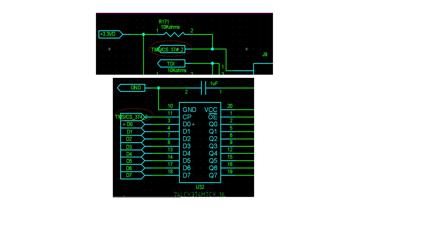
the the 10Kohm pullup resistor at the TMS pin, we can see a glitch at the at TMS pin voltage waveform during Vcc rising.
the datasheet descripes TMS pin has internal pullup circuit, so why there is a low status during chip POR, thanks.
Hardy,
Is the internal VREG being used in this design? Please see the NOTE immediately preceding "Table 4-1 Signal Descriptions" in the Datasheet. I have included it below. If the internal VREG, this is expected behavior. If this is unacceptable, follow the instructions in the note.
If the note above does not address the concern, I see that the naming convention of the TMS signal is "TMS/CS.." Would this indicate a usage as a GPIO during normal operation? Is it connected toexternal circuitry that could be pulling it low during POR?
Regards,
Mark