


Part Number: TMS320F28379D
Other Parts Discussed in Thread: CONTROLSUITE
Hi,
I am trying to perform SPI communication between F28379D launchpad (Master) and F28379D ControlCard (Slave). I have written the code following the SPI loopback example shipped in ControlSuite. I configure the master to send a counter data continuously over SPI and slave is configured to read the received data continuously. During transmit I ensure TXFFST is empty before placing the new data on SPITXBUF and while receiving I will check RXFFST if new data is available before reading the data from SPIRXBUF.
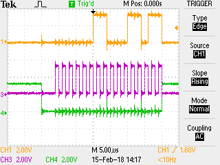
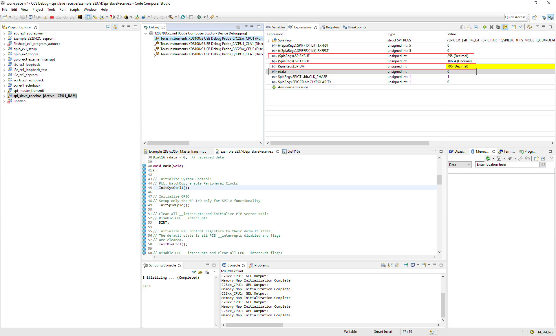
When I configure both master and slave either as rising edge-no delay or as falling edge-delay half cycle clock modes, I can see the data is received properly in slave. But if I configure both master and slave either as rising edge-half cycle delay or as falling edge-no delay, I am not able to read properly from SPIRXBUF. In these cases, SPIDAT is updated by the received data regularly but the data from SPIDAT is not loaded properly into SPIRXBUF and RXFFST is zero (attached snapshot). Also the SIMO data along with clock and CS is present and can be confirmed using CRO (attached screenshot) and the SIMO data observed in CRO matches with the data observed in SPIDAT.
If I replace the slave with other board like F28075 i can see the data being received properly in SPIRXBUF. Can you check once and let me know the reason for this issue? I have attached the code used for both master and slave for the reference.
Thanks,
Aditya
SPI Master
//###########################################################################
// FILE:   Example_2837xDSpi_MasterTransmit.c
// TITLE:  Transmit Tx data from SPI master
//
//!  This program transmits data from SPI master continuously. This program is configured to use on
//!  F28379D Launchpad with modification for system clock and SPi pins.
//!
//!  A stream of data is sent.
//!  The sent data looks like this: \n
//!  0000 0001 0002 0003 0004 0005 0006 0007 .... FFFE FFFF \n
//!  This pattern is repeated forever.
//!
//!  \b Watch \b Variables \n
//!  - \b sdata - sent data

#include "F28x_Project.h"     // Device Headerfile and Examples Include File

// Function prototype
void delay_loop(void);
void spi_xmit(Uint16 a);
void spi_fifo_init(void);
void spi_init(void);
void InitSpiaGpio(void);
void InitSysCtrl1(void);

Uint16 sdata = 0;  // send data

void main(void)
{
// Initialize System Control
// PLL, WatchDog, enable Peripheral Clocks
   InitSysCtrl1();

// Initialize GPIO
   InitSpiaGpio();

// Clear all __interrupts and initialize PIE vector table
// Disable CPU __interrupts
   DINT;

// Initialize PIE control registers to their default state.
// The default state is all PIE __interrupts disabled and flags
// are cleared.
   InitPieCtrl();

// Disable CPU __interrupts and clear all CPU __interrupt flags:
   IER = 0x0000;
   IFR = 0x0000;

// Initialize the PIE vector table with pointers to the shell Interrupt
// Service Routines (ISR).
// This will populate the entire table, even if the __interrupt
// is not used in this example.
   InitPieVectTable();

// Initialize the Device Peripherals
   spi_fifo_init();	  // Initialize the Spi FIFO
   spi_init();		  // init SPI

// Transmit the data continuously
// Interrupts are not used in this example.
   sdata = 0x0000;
   for(;;)
   {
     // Transmit data
     spi_xmit(sdata);
     delay_loop();
     sdata++;
   }
}

// Local Interrupt Service Routines (ISRs) and functions

void delay_loop()
{
    long      i;
    for (i = 0; i < 1000000; i++) {}
}

void InitSysCtrl1(void)
{
    // Disable the watchdog
    DisableDog();

#ifdef _FLASH
// Copy time critical code and Flash setup code to RAM
// This includes the following functions:  InitFlash();
// The  RamfuncsLoadStart, RamfuncsLoadSize, and RamfuncsRunStart
// symbols are created by the linker. Refer to the device .cmd file.
    memcpy(&RamfuncsRunStart, &RamfuncsLoadStart, (size_t)&RamfuncsLoadSize);

// Call Flash Initialization to setup flash waitstates
// This function must reside in RAM
    InitFlash();
#endif

    // *IMPORTANT*
    // The Device_cal function, which copies the ADC & oscillator calibration values
    // from TI reserved OTP into the appropriate trim registers, occurs automatically
    // in the Boot ROM. If the boot ROM code is bypassed during the debug process, the
    // following function MUST be called for the ADC and oscillators to function according
    // to specification. The clocks to the ADC MUST be enabled before calling this
    // function.
    // See the device data manual and/or the ADC Reference
    // Manual for more information.
#ifdef CPU1
    EALLOW;

    //enable pull-ups on unbonded IOs as soon as possible to reduce power consumption.
    GPIO_EnableUnbondedIOPullups();

    CpuSysRegs.PCLKCR13.bit.ADC_A = 1;
    CpuSysRegs.PCLKCR13.bit.ADC_B = 1;
    CpuSysRegs.PCLKCR13.bit.ADC_C = 1;
    CpuSysRegs.PCLKCR13.bit.ADC_D = 1;

    //check if device is trimmed
    if(*((Uint16 *)0x5D1B6) == 0x0000){
        //device is not trimmed, apply static calibration values
        AnalogSubsysRegs.ANAREFTRIMA.all = 31709;
        AnalogSubsysRegs.ANAREFTRIMB.all = 31709;
        AnalogSubsysRegs.ANAREFTRIMC.all = 31709;
        AnalogSubsysRegs.ANAREFTRIMD.all = 31709;
    }

    CpuSysRegs.PCLKCR13.bit.ADC_A = 0;
    CpuSysRegs.PCLKCR13.bit.ADC_B = 0;
    CpuSysRegs.PCLKCR13.bit.ADC_C = 0;
    CpuSysRegs.PCLKCR13.bit.ADC_D = 0;
    EDIS;

    // Initialize the PLL control: PLLCR and CLKINDIV
    // F28_PLLCR and F28_CLKINDIV are defined in F2837xD_Examples.h
    // Note: The internal oscillator CANNOT be used as the PLL source if the
    // PLLSYSCLK is configured to frequencies above 194 MHz.
    InitSysPll(XTAL_OSC,40,FMULT_0,PLLCLK_BY_2);      //PLLSYSCLK = (XTAL_OSC) * (IMULT + FMULT) / (PLLSYSCLKDIV)
#endif

    //Turn on all peripherals
    InitPeripheralClocks();
}
void spi_init()
{
	SpiaRegs.SPICCR.bit.SPISWRESET = 0;          // Reset on
    SpiaRegs.SPICCR.bit.SPICHAR = 15;            // 16-bit char bits
    SpiaRegs.SPICCR.bit.CLKPOLARITY = 0;         // rising edge
    SpiaRegs.SPICCR.bit.SPILBK = 0;              // Loopback disabled

	SpiaRegs.SPIBRR.all =0x0063;                 // baud rate setting for master

	SpiaRegs.SPICTL.bit.TALK = 1;                // enable talk
	SpiaRegs.SPICTL.bit.SPIINTENA = 0;           // SPI int disabled
    SpiaRegs.SPICTL.bit.MASTER_SLAVE = 1;        // Master mode
    SpiaRegs.SPICTL.bit.CLK_PHASE = 1;           // delay half cycle

    SpiaRegs.SPICCR.bit.SPISWRESET = 1;          // Relinquish SPI from Reset
    SpiaRegs.SPIPRI.bit.FREE = 1;                // Set so breakpoints don't disturb xmission
}

void spi_xmit(Uint16 a)
{
    if (SpiaRegs.SPIFFTX.bit.TXFFST < 16) {  //Check if TX fifo is empty before sending the data
        SpiaRegs.SPITXBUF = a;
    }
}

void spi_fifo_init()
{
// Initialize SPI TX FIFO registers for now
    SpiaRegs.SPIFFTX.bit.SPIFFENA = 1;    // Enable SPI fifo
    SpiaRegs.SPIFFTX.bit.TXFIFO = 1;      // Enable Tx fifo
    SpiaRegs.SPIFFTX.bit.TXFFIL = 0;      // Tx fifo level is zero
    SpiaRegs.SPIFFTX.bit.TXFFIENA = 0;    // Disable tx fifo interrupt
    SpiaRegs.SPIFFTX.bit.TXFFINTCLR = 1;  // clear tx interrupt flag
    SpiaRegs.SPIFFTX.bit.SPIRST = 1;      // release SPI fifo TX
    SpiaRegs.SPIFFCT.all=0x0;             // TX delay = 0
}

void InitSpiaGpio()
{

   EALLOW;

/* Enable internal pull-up for the selected pins */
// Pull-ups can be enabled or disabled by the user.
// This will enable the pullups for the specified pins.

    GpioCtrlRegs.GPBPUD.bit.GPIO58 = 0;   // Enable pull-up on GPIO58 (SPISIMOA)
    GpioCtrlRegs.GPBPUD.bit.GPIO59 = 0;   // Enable pull-up on GPIO59 (SPISOMIA)
    GpioCtrlRegs.GPBPUD.bit.GPIO60 = 0;   // Enable pull-up on GPIO60 (SPICLKA)
    GpioCtrlRegs.GPBPUD.bit.GPIO61 = 0;   // Enable pull-up on GPIO61 (SPISTEA)

/* Set qualification for selected pins to asynch only */
// This will select asynch (no qualification) for the selected pins.

    GpioCtrlRegs.GPBQSEL2.bit.GPIO58 = 3; // Asynch input GPIO58 (SPISIMOA)
    GpioCtrlRegs.GPBQSEL2.bit.GPIO59 = 3; // Asynch input GPIO59 (SPISOMIA)
    GpioCtrlRegs.GPBQSEL2.bit.GPIO60 = 3; // Asynch input GPIO60 (SPICLKA)
    GpioCtrlRegs.GPBQSEL2.bit.GPIO61 = 3; // Asynch input GPIO61 (SPISTEA)

/* Configure SPI-A pins using GPIO regs*/
// This specifies which of the possible GPIO pins will be SPI functional pins.

    GpioCtrlRegs.GPBMUX2.bit.GPIO58 = 3; // Configure GPIO58 as SPISIMOA
    GpioCtrlRegs.GPBMUX2.bit.GPIO59 = 3; // Configure GPIO59 as SPISOMIA
    GpioCtrlRegs.GPBMUX2.bit.GPIO60 = 3; // Configure GPIO60 as SPICLKA
    GpioCtrlRegs.GPBMUX2.bit.GPIO61 = 3; // Configure GPIO61 as SPISTEA

    GpioCtrlRegs.GPBGMUX2.bit.GPIO58 = 3; // Configure GPIO58 as SPISIMOA
    GpioCtrlRegs.GPBGMUX2.bit.GPIO59 = 3; // Configure GPIO59 as SPISOMIA
    GpioCtrlRegs.GPBGMUX2.bit.GPIO60 = 3; // Configure GPIO60 as SPICLKA
    GpioCtrlRegs.GPBGMUX2.bit.GPIO61 = 3; // Configure GPIO61 as SPISTEA

    EDIS;
}

//===========================================================================
// No more.
//===========================================================================
SPI Slave
//###########################################################################
// FILE:   Example_2837xDSpi_Slavereceive.c
// TITLE:  Receive data from SPI master as slave
//
//!  This program receive data from SPI master continuously. This program is configured to use on
//!  F28379D ControlCard.
//!
//!  A stream of data is received.
//!  The received data looks like this: \n
//!  0000 0001 0002 0003 0004 0005 0006 0007 .... FFFE FFFF \n
//!  This pattern is repeated forever.
//!
//!  \b Watch \b Variables \n
//!  - \b rdata - received data

#include "F28x_Project.h"     // Device Headerfile and Examples Include File

// Function prototypes
void delay_loop(void);
void spi_fifo_init(void);
void spi_init(void);
void error(void);
void InitSysCtrl1(void);
void InitSpiaGpio(void);

Uint16 rdata = 0;  // received data

void main(void)
{

// Initialize System Control:
// PLL, WatchDog, enable Peripheral Clocks
   InitSysCtrl1();

// Initialize GPIO
// Setup only the GP I/O only for SPI-A functionality
   InitSpiaGpio();

// Clear all __interrupts and initialize PIE vector table
// Disable CPU __interrupts
   DINT;

// Initialize PIE control registers to their default state.
// The default state is all PIE __interrupts disabled and flags
// are cleared.
   InitPieCtrl();

// Disable CPU __interrupts and clear all CPU __interrupt flags:
   IER = 0x0000;
   IFR = 0x0000;

// Initialize the PIE vector table with pointers to the shell Interrupt
// Service Routines (ISR).
// This will populate the entire table, even if the __interrupt
// is not used in this example.
   InitPieVectTable();

// Initialize the Device Peripherals
   spi_fifo_init();	  // Initialize the Spi FIFO
   spi_init();		  // init SPI

// Receive data from master continuously
   for(;;)
   {
       if(SpiaRegs.SPIFFRX.bit.RXFFST >= 1){
       //if(SpiaRegs.SPISTS.bit.INT_FLAG == 1){
           rdata = SpiaRegs.SPIRXBUF;
       }
   }
}

// Local Interrupt Service Routines (ISRs) and functions

void delay_loop()
{
    long      i;
    for (i = 0; i < 1000000; i++) {}
}

void InitSysCtrl1(void)
{
    // Disable the watchdog
    DisableDog();

#ifdef _FLASH
// Copy time critical code and Flash setup code to RAM
// This includes the following functions:  InitFlash();
// The  RamfuncsLoadStart, RamfuncsLoadSize, and RamfuncsRunStart
// symbols are created by the linker. Refer to the device .cmd file.
    memcpy(&RamfuncsRunStart, &RamfuncsLoadStart, (size_t)&RamfuncsLoadSize);

// Call Flash Initialization to setup flash waitstates
// This function must reside in RAM
    InitFlash();
#endif

    // *IMPORTANT*
    // The Device_cal function, which copies the ADC & oscillator calibration values
    // from TI reserved OTP into the appropriate trim registers, occurs automatically
    // in the Boot ROM. If the boot ROM code is bypassed during the debug process, the
    // following function MUST be called for the ADC and oscillators to function according
    // to specification. The clocks to the ADC MUST be enabled before calling this
    // function.
    // See the device data manual and/or the ADC Reference
    // Manual for more information.
#ifdef CPU1
    EALLOW;

    //enable pull-ups on unbonded IOs as soon as possible to reduce power consumption.
    GPIO_EnableUnbondedIOPullups();

    CpuSysRegs.PCLKCR13.bit.ADC_A = 1;
    CpuSysRegs.PCLKCR13.bit.ADC_B = 1;
    CpuSysRegs.PCLKCR13.bit.ADC_C = 1;
    CpuSysRegs.PCLKCR13.bit.ADC_D = 1;

    //check if device is trimmed
    if(*((Uint16 *)0x5D1B6) == 0x0000){
        //device is not trimmed, apply static calibration values
        AnalogSubsysRegs.ANAREFTRIMA.all = 31709;
        AnalogSubsysRegs.ANAREFTRIMB.all = 31709;
        AnalogSubsysRegs.ANAREFTRIMC.all = 31709;
        AnalogSubsysRegs.ANAREFTRIMD.all = 31709;
    }

    CpuSysRegs.PCLKCR13.bit.ADC_A = 0;
    CpuSysRegs.PCLKCR13.bit.ADC_B = 0;
    CpuSysRegs.PCLKCR13.bit.ADC_C = 0;
    CpuSysRegs.PCLKCR13.bit.ADC_D = 0;
    EDIS;

    // Initialize the PLL control: PLLCR and CLKINDIV
    // F28_PLLCR and F28_CLKINDIV are defined in F2837xD_Examples.h
    // Note: The internal oscillator CANNOT be used as the PLL source if the
    // PLLSYSCLK is configured to frequencies above 194 MHz.
    InitSysPll(XTAL_OSC,IMULT_20,FMULT_0,PLLCLK_BY_2);      //PLLSYSCLK = (XTAL_OSC) * (IMULT + FMULT) / (PLLSYSCLKDIV)
#endif

    //Turn on all peripherals
    InitPeripheralClocks();
}

void spi_init()
{
    SpiaRegs.SPICCR.bit.SPISWRESET = 0;          // Reset on
    SpiaRegs.SPICCR.bit.SPICHAR = 15;            // 16-bit char bits
    SpiaRegs.SPICCR.bit.CLKPOLARITY = 0;         // rising edge
    SpiaRegs.SPICCR.bit.SPILBK = 0;              // Loopback disabled

    //SpiaRegs.SPIBRR.all =0x0063;                 // baud rate setting not required for slave

    SpiaRegs.SPICTL.bit.TALK = 1;                // enable talk
    SpiaRegs.SPICTL.bit.SPIINTENA = 0;           // SPI int disabled
    SpiaRegs.SPICTL.bit.MASTER_SLAVE = 0;        // Slave mode
    SpiaRegs.SPICTL.bit.CLK_PHASE = 1;           // delay half cycle

    SpiaRegs.SPICCR.bit.SPISWRESET = 1;          // Relinquish SPI from Reset
    SpiaRegs.SPIPRI.bit.FREE = 1;                // Set so breakpoints don't disturb xmission
}

void spi_fifo_init()
{
// Initialize SPI RX FIFO registers
    SpiaRegs.SPIFFTX.bit.SPIFFENA = 1;    // Enable SPI fifo
    SpiaRegs.SPIFFRX.bit.RXFFIENA = 0;    //Disable RX FIFO interrupt
    SpiaRegs.SPIFFRX.bit.RXFFIL = 16;
    SpiaRegs.SPIFFRX.bit.RXFFINTCLR = 1;  //Clear RX Interrupt flag
    SpiaRegs.SPIFFRX.bit.RXFIFORESET = 1; // Release RX FIFO from reset
}

void InitSpiaGpio()
{

   EALLOW;

/* Enable internal pull-up for the selected pins */
// Pull-ups can be enabled or disabled by the user.
// This will enable the pullups for the specified pins.

    GpioCtrlRegs.GPAPUD.bit.GPIO16 = 0;   // Enable pull-up on GPIO16 (SPISIMOA)
    GpioCtrlRegs.GPAPUD.bit.GPIO17 = 0;   // Enable pull-up on GPIO17 (SPISOMIA)
    GpioCtrlRegs.GPAPUD.bit.GPIO18 = 0;   // Enable pull-up on GPIO18 (SPICLKA)
    GpioCtrlRegs.GPAPUD.bit.GPIO19 = 0;   // Enable pull-up on GPIO19 (SPISTEA)

/* Set qualification for selected pins to asynch only */
// This will select asynch (no qualification) for the selected pins.

    GpioCtrlRegs.GPAQSEL2.bit.GPIO16 = 3; // Asynch input GPIO16 (SPISIMOA)
    GpioCtrlRegs.GPAQSEL2.bit.GPIO17 = 3; // Asynch input GPIO17 (SPISOMIA)
    GpioCtrlRegs.GPAQSEL2.bit.GPIO18 = 3; // Asynch input GPIO18 (SPICLKA)
    GpioCtrlRegs.GPAQSEL2.bit.GPIO19 = 3; // Asynch input GPIO19 (SPISTEA)

/* Configure SPI-A pins using GPIO regs*/
// This specifies which of the possible GPIO pins will be SPI functional pins.

    GpioCtrlRegs.GPAMUX2.bit.GPIO16 = 1; // Configure GPIO16 as SPISIMOA
    GpioCtrlRegs.GPAMUX2.bit.GPIO17 = 1; // Configure GPIO17 as SPISOMIA
    GpioCtrlRegs.GPAMUX2.bit.GPIO18 = 1; // Configure GPIO18 as SPICLKA
    GpioCtrlRegs.GPAMUX2.bit.GPIO19 = 1; // Configure GPIO19 as SPISTEA

    EDIS;
}
//===========================================================================
// No more.
//===========================================================================
