Hi,
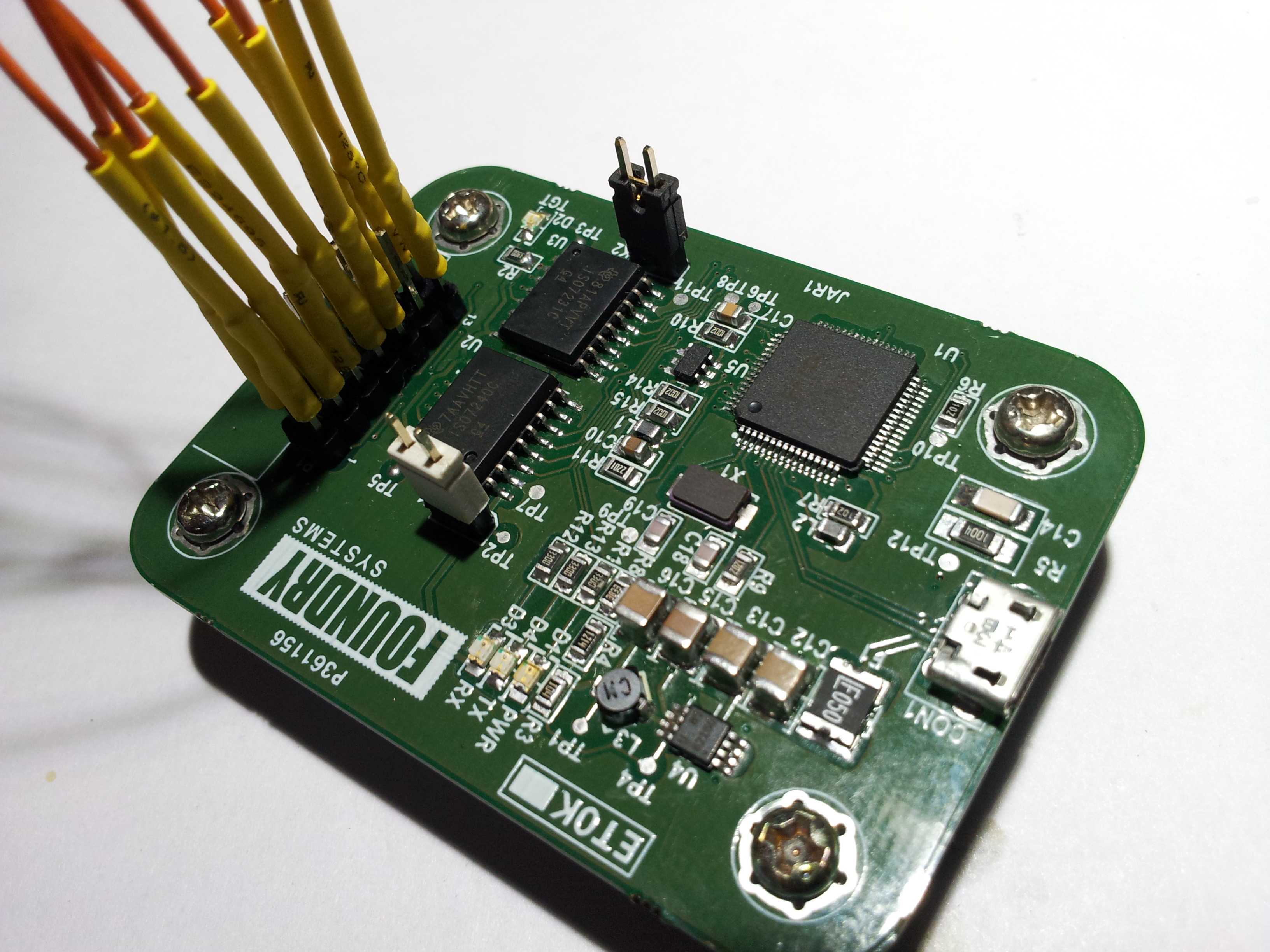
As part of a project, wanted to have only the Piccolo alone on a standalone board to simplify the project; the FT2232 Programmer/debugger had to be broken out to program the controller. This resulted in two small PCB's of which the controller board alone is of interest while the programmer/debugger board came out due to absolute necessity of programming the controller. Attached pictures of both PCB's.
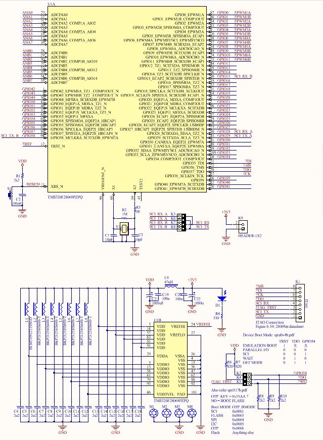
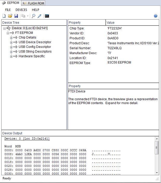
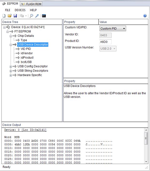
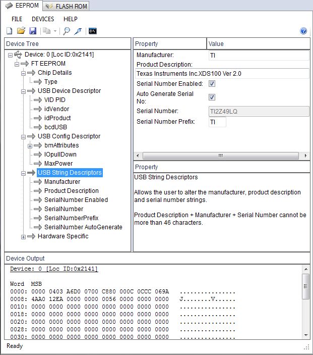
I've tried to copy the EEPROM contents from the LAUNCHXL_F28069M to the programmer board to make it as identical to the launchpad to avoid any hassles in programming/debugging the controller during production phase of the final project. Attached schematics of both boards.

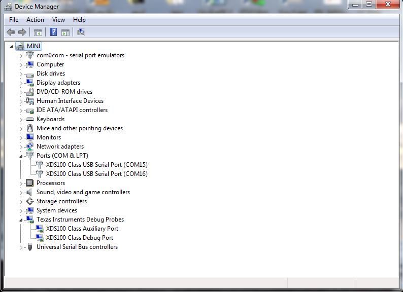
After copying the VID, PID and the rest of the EEPROM contents, the programmer identifies itself as a XDS100 V2 debugger, as in the case with the launchpad. Attached screenshots.

Trying to do a test connection, attached log:
[Start: Texas Instruments XDS100v2 USB Debug Probe_0]

Execute the command:

%ccs_base%/common/uscif/dbgjtag -f %boarddatafile% -rv -o -F inform,logfile=yes -S pathlength -S integrity

[Result]


-----[Print the board config pathname(s)]------------------------------------

C:\Users\Manu\AppData\Local\TEXASI~1\CCS\
    ti\4\0\BrdDat\testBoard.dat

-----[Print the reset-command software log-file]-----------------------------

This utility has selected a 100- or 510-class product.
This utility will load the adapter 'jioserdesusb.dll'.
The library build date was 'Feb  8 2018'.
The library build time was '18:36:28'.
The library package version is '7.0.188.0'.
The library component version is '35.35.0.0'.
The controller does not use a programmable FPGA.
The controller has a version number of '4' (0x00000004).
The controller has an insertion length of '0' (0x00000000).
This utility will attempt to reset the controller.
This utility has successfully reset the controller.

-----[Print the reset-command hardware log-file]-----------------------------

The scan-path will be reset by toggling the JTAG TRST signal.
The controller is the FTDI FT2232 with USB interface.
The link from controller to target is direct (without cable).
The software is configured for FTDI FT2232 features.
The controller cannot monitor the value on the EMU[0] pin.
The controller cannot monitor the value on the EMU[1] pin.
The controller cannot control the timing on output pins.
The controller cannot control the timing on input pins.
The scan-path link-delay has been set to exactly '0' (0x0000).

-----[The log-file for the JTAG TCLK output generated from the PLL]----------

There is no hardware for programming the JTAG TCLK frequency.

-----[Measure the source and frequency of the final JTAG TCLKR input]--------

There is no hardware for measuring the JTAG TCLK frequency.

-----[Perform the standard path-length test on the JTAG IR and DR]-----------

This path-length test uses blocks of 64 32-bit words.

The test for the JTAG IR instruction path-length succeeded.
The JTAG IR instruction path-length is 38 bits.

The test for the JTAG DR bypass path-length succeeded.
The JTAG DR bypass path-length is 1 bits.

-----[Perform the Integrity scan-test on the JTAG IR]------------------------

This test will use blocks of 64 32-bit words.
This test will be applied just once.

Do a test using 0xFFFFFFFF.
Scan tests: 1, skipped: 0, failed: 0
Do a test using 0x00000000.
Scan tests: 2, skipped: 0, failed: 0
Do a test using 0xFE03E0E2.
Scan tests: 3, skipped: 0, failed: 0
Do a test using 0x01FC1F1D.
Scan tests: 4, skipped: 0, failed: 0
Do a test using 0x5533CCAA.
Scan tests: 5, skipped: 0, failed: 0
Do a test using 0xAACC3355.
Scan tests: 6, skipped: 0, failed: 0
All of the values were scanned correctly.

The JTAG IR Integrity scan-test has succeeded.

-----[Perform the Integrity scan-test on the JTAG DR]------------------------

This test will use blocks of 64 32-bit words.
This test will be applied just once.

Do a test using 0xFFFFFFFF.
Scan tests: 1, skipped: 0, failed: 0
Do a test using 0x00000000.
Scan tests: 2, skipped: 0, failed: 0
Do a test using 0xFE03E0E2.
Scan tests: 3, skipped: 0, failed: 0
Do a test using 0x01FC1F1D.
Scan tests: 4, skipped: 0, failed: 0
Do a test using 0x5533CCAA.
Scan tests: 5, skipped: 0, failed: 0
Do a test using 0xAACC3355.
Scan tests: 6, skipped: 0, failed: 0
All of the values were scanned correctly.

The JTAG DR Integrity scan-test has succeeded.

[End: Texas Instruments XDS100v2 USB Debug Probe_0]
Trying to debug the default test application, Code Composer Studio states that the device is held in Reset, attached log:
C28xx: Failed CPU Reset: (Error -1137 @ 0x6) Device is held in reset. Take the device out of reset, and retry the operation. (Emulation package 7.0.188.0)
C28xx: Trouble Reading Register PC: (Error -1137 @ 0x0) Device is held in reset. Take the device out of reset, and retry the operation. (Emulation package 7.0.188.0)
C28xx: Trouble Reading Register ST1: (Error -1137 @ 0x6) Device is held in reset. Take the device out of reset, and retry the operation. (Emulation package 7.0.188.0)
C28xx: GEL: Error while executing OnReset(1): Target failed to read register ST1
	 at (ST1&~(0x0100)) [f28069.gel:312]
	 at C28x_Mode() [f28069.gel:32]
	 at OnReset(1)
C28xx: Flash Programmer: Warning: The configured device (TMS320F28069), does not match the detected device (). Flash Programming operations could be affected. Please consider modifying your target configuration file.
C28xx: Failed CPU Reset: (Error -1137 @ 0x0) Device is held in reset. Take the device out of reset, and retry the operation. (Emulation package 7.0.188.0)
C28xx: Trouble Reading Register PC: (Error -1137 @ 0x0) Device is held in reset. Take the device out of reset, and retry the operation. (Emulation package 7.0.188.0)
C28xx: Trouble Reading Register ST1: (Error -1137 @ 0x6) Device is held in reset. Take the device out of reset, and retry the operation. (Emulation package 7.0.188.0)
C28xx: GEL: Error while executing OnReset(1): Target failed to read register ST1
	 at (ST1&~(0x0100)) [f28069.gel:312]
	 at C28x_Mode() [f28069.gel:32]
	 at OnReset(1)
C28xx: Trouble Writing Memory Block at 0xae0 on Page 1 of Length 0x1: (Error -1137 @ 0xAE1) Device is held in reset. Take the device out of reset, and retry the operation. (Emulation package 7.0.188.0)
C28xx: Error occurred during flash operation: Target failed to write 0x00000AE0@Data
C28xx: Trouble Writing Memory Block at 0xae1 on Page 1 of Length 0x1: (Error -1137 @ 0xAE2) Device is held in reset. Take the device out of reset, and retry the operation. (Emulation package 7.0.188.0)
C28xx: Error occurred during flash operation: Target failed to write 0x00000AE1@Data
C28xx: Trouble Writing Memory Block at 0xae2 on Page 1 of Length 0x1: (Error -1137 @ 0xAE3) Device is held in reset. Take the device out of reset, and retry the operation. (Emulation package 7.0.188.0)
C28xx: Error occurred during flash operation: Target failed to write 0x00000AE2@Data
C28xx: Trouble Writing Memory Block at 0xae3 on Page 1 of Length 0x1: (Error -1137 @ 0xAE4) Device is held in reset. Take the device out of reset, and retry the operation. (Emulation package 7.0.188.0)
C28xx: Error occurred during flash operation: Target failed to write 0x00000AE3@Data
C28xx: Trouble Writing Memory Block at 0xae4 on Page 1 of Length 0x1: (Error -1137 @ 0xAE5) Device is held in reset. Take the device out of reset, and retry the operation. (Emulation package 7.0.188.0)
C28xx: Error occurred during flash operation: Target failed to write 0x00000AE4@Data
C28xx: Trouble Writing Memory Block at 0xae5 on Page 1 of Length 0x1: (Error -1137 @ 0xAE6) Device is held in reset. Take the device out of reset, and retry the operation. (Emulation package 7.0.188.0)
C28xx: Error occurred during flash operation: Target failed to write 0x00000AE5@Data
C28xx: Trouble Writing Memory Block at 0xae6 on Page 1 of Length 0x1: (Error -1137 @ 0xAE7) Device is held in reset. Take the device out of reset, and retry the operation. (Emulation package 7.0.188.0)
C28xx: Error occurred during flash operation: Target failed to write 0x00000AE6@Data
C28xx: Trouble Writing Memory Block at 0xae7 on Page 1 of Length 0x1: (Error -1137 @ 0xAE8) Device is held in reset. Take the device out of reset, and retry the operation. (Emulation package 7.0.188.0)
C28xx: Error occurred during flash operation: Target failed to write 0x00000AE7@Data
C28xx: Flash Programmer: Device is locked or not connected. Operation cancelled.
C28xx: File Loader: Memory write failed: Unknown error
C28xx: GEL: File: C:\Users\Manu\workspace_v8\Example_2806xLaunchPad\Debug\Example_2806xLaunchPad.out: Load failed.
Measuring the voltage on Pin #11/XRS_N (RESET#) shows that the controller is held at 0V, which would explain the logs. I wonder why how I can take the device out of Reset. Maybe I've missed out something. Can someone be kind enough to pint out the issue at hand ?
Thanks,
Manu