This thread has been locked.
If you have a related question, please click the "Ask a related question" button in the top right corner. The newly created question will be automatically linked to this question.
Hi
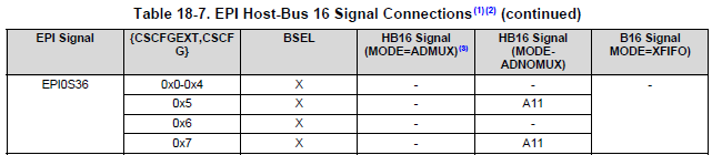
I use the F28M35 to connet 2 SRAM base on the EPI-16-bit Host Mode。
I don't know how configurate some espiecial pin.
For example, EPI0S36 ----A11------PB7_GPIO15
at the hw_gpio.h
#define GPIO_PCTL_PB7_M 0xF0000000 // PB7 mask
#define GPIO_PCTL_PB7_NMI 0x40000000 // NMI on PB7
#define GPIO_PCTL_PB7_MIIRXD1 0x70000000 // EMAC MIIRXD1 on PB7
#define GPIO_PCTL_PB7_I2C0SCL 0xD0000000 // I2C0SCL on PB7
#define GPIO_PCTL_PB7_U1RX 0xE0000000 // U1RX on PB7
#define GPIO_PCTL_PB7_SSI1FSS 0xF0000000 // SSI1FSS on PB7
there are not the definition as below;
#define GPIO_PCTL_PB5_EPI0S22 0x00800000 // EPI0S22 on PB5
thank you for you reply . I have done the suggest which you tall me;
HWREG(GPIO_PORTB_BASE + GPIO_O_PCTL) = GPIO_PCTL_PB4_EPI0S23 |
GPIO_PCTL_PB5_EPI0S22|
GPIO_PCTL_PB6_EPI0S37|
GPIO_PCTL_PB7_EPI0S36;
the other pin is also do by this, but it does not work well .the follow is my project based on the "epi_sram_8bit.c"which is found in the control SUITE。 The problem is that I can't read or write in the sram.
My desire of sram is based on the table 5-49 in the F28M35x Concerto™ Microcontrollers .
int
main(void)
{
// Disable Protection
HWREG(SYSCTL_MWRALLOW) = 0xA5A5A5A5;
// Setup main clock tree for 75MHz - M3 and 150MHz - C28x
SysCtlClockConfigSet(SYSCTL_SYSDIV_1 | SYSCTL_M3SSDIV_2 | SYSCTL_USE_PLL |
(SYSCTL_SPLLIMULT_M & 0x0F));
#ifdef _FLASH
// Copy time critical code and Flash setup code to RAM
// This includes the following functions: InitFlash();
// The RamfuncsLoadStart, RamfuncsLoadSize, and RamfuncsRunStart
// symbols are created by the linker. Refer to the device .cmd file.
memcpy(&RamfuncsRunStart, &RamfuncsLoadStart, (size_t)&RamfuncsLoadSize);
// Call Flash Initialization to setup flash waitstates
// This function must reside in RAM
FlashInit();
#endif
// Enable Clock for EPI & GPIO Ports
SysCtlPeripheralEnable(SYSCTL_PERIPH_EPI0);
SysCtlPeripheralEnable(SYSCTL_PERIPH_GPIOB);
SysCtlPeripheralEnable(SYSCTL_PERIPH_GPIOC);
SysCtlPeripheralEnable(SYSCTL_PERIPH_GPIOD);
SysCtlPeripheralEnable(SYSCTL_PERIPH_GPIOE);
SysCtlPeripheralEnable(SYSCTL_PERIPH_GPIOF);
SysCtlPeripheralEnable(SYSCTL_PERIPH_GPIOG);
SysCtlPeripheralEnable(SYSCTL_PERIPH_GPIOH);
SysCtlPeripheralEnable(SYSCTL_PERIPH_GPIOJ);
// Configure the GPIO setting for the EPI pins.
SetPortControl();
GPIODirModeSet(GPIO_PORTB_BASE,
(GPIO_PIN_4 | GPIO_PIN_5|GPIO_PIN_6|GPIO_PIN_7),
GPIO_DIR_MODE_HW);
GPIOPadConfigSet(GPIO_PORTB_BASE,
(GPIO_PIN_4 | GPIO_PIN_5|GPIO_PIN_6|GPIO_PIN_7),
GPIO_PIN_TYPE_STD_WPU);
GPIODirModeSet(GPIO_PORTC_BASE,
(GPIO_PIN_4 | GPIO_PIN_5 | GPIO_PIN_6 | GPIO_PIN_7),
GPIO_DIR_MODE_HW);
GPIOPadConfigSet(GPIO_PORTC_BASE,
(GPIO_PIN_4 | GPIO_PIN_5 | GPIO_PIN_6 | GPIO_PIN_7),
GPIO_PIN_TYPE_STD_WPU);
GPIODirModeSet(GPIO_PORTD_BASE,
(GPIO_PIN_2 | GPIO_PIN_3|GPIO_PIN_7),
GPIO_DIR_MODE_HW);
GPIOPadConfigSet(GPIO_PORTD_BASE,
(GPIO_PIN_2 | GPIO_PIN_3|GPIO_PIN_7),
GPIO_PIN_TYPE_STD_WPU);
GPIODirModeSet(GPIO_PORTE_BASE,
(GPIO_PIN_0 | GPIO_PIN_1 | GPIO_PIN_2 | GPIO_PIN_3|GPIO_PIN_4|GPIO_PIN_5),
GPIO_DIR_MODE_HW);
GPIOPadConfigSet(GPIO_PORTE_BASE,
(GPIO_PIN_0 | GPIO_PIN_1 | GPIO_PIN_2 | GPIO_PIN_3|GPIO_PIN_4|GPIO_PIN_5),
GPIO_PIN_TYPE_STD_WPU);
GPIODirModeSet(GPIO_PORTF_BASE,
(GPIO_PIN_4 | GPIO_PIN_5|GPIO_PIN_6),
GPIO_DIR_MODE_HW);
GPIOPadConfigSet(GPIO_PORTF_BASE,
(GPIO_PIN_4 | GPIO_PIN_5|GPIO_PIN_6),
GPIO_PIN_TYPE_STD_WPU);
GPIODirModeSet(GPIO_PORTG_BASE,
(GPIO_PIN_0 | GPIO_PIN_1|GPIO_PIN_2|GPIO_PIN_5|GPIO_PIN_6),
GPIO_DIR_MODE_HW);
GPIOPadConfigSet(GPIO_PORTG_BASE,
(GPIO_PIN_0 | GPIO_PIN_1|GPIO_PIN_2|GPIO_PIN_5|GPIO_PIN_6),
GPIO_PIN_TYPE_STD_WPU);
GPIODirModeSet(GPIO_PORTH_BASE,
(GPIO_PIN_0 | GPIO_PIN_1 | GPIO_PIN_2 | GPIO_PIN_3 |
GPIO_PIN_4 | GPIO_PIN_5 | GPIO_PIN_6 | GPIO_PIN_7),
GPIO_DIR_MODE_HW);
GPIOPadConfigSet(GPIO_PORTH_BASE,
(GPIO_PIN_0 | GPIO_PIN_1 | GPIO_PIN_2 | GPIO_PIN_3 |
GPIO_PIN_4 | GPIO_PIN_5 | GPIO_PIN_6 | GPIO_PIN_7),
GPIO_PIN_TYPE_STD_WPU);
GPIODirModeSet(GPIO_PORTJ_BASE,
(GPIO_PIN_0 | GPIO_PIN_1 | GPIO_PIN_2 | GPIO_PIN_3 |
GPIO_PIN_4 | GPIO_PIN_5 ),
GPIO_DIR_MODE_HW);
GPIOPadConfigSet(GPIO_PORTJ_BASE,
(GPIO_PIN_0 | GPIO_PIN_1 | GPIO_PIN_2 | GPIO_PIN_3 |
GPIO_PIN_4 | GPIO_PIN_5 ),
GPIO_PIN_TYPE_STD_WPU);
// Use EPI31 like GPIO and connect it to A20 pin of Memory.
// GPIOPinTypeGPIOOutput(GPIO_PORTG_BASE, GPIO_PIN_7);
// GPIOPinWrite(GPIO_PORTG_BASE, GPIO_PIN_7, GPIO_PIN_7);
// Set 16 Bit HostBus mode.
EPIModeSet(EPI0_BASE, EPI_MODE_HB16);
//Set clock divider to 1 (divide by 2). With this EPI Frq will be 37.5MHz (M3-Frq/2).
EPIDividerSet(EPI0_BASE, 0x2);
// Read wait state = 0
// Write wait state = 0
// Address & Data are not muxed (ADNOMUX = 0x1).
EPIModeSet(EPI0_BASE,EPI_MODE_HB16);
EPIConfigHB16Set(EPI0_BASE, (EPI_HB16_MODE_ADDEMUX | EPI_HB16_WRWAIT_0|EPI_HB16_BSEL | EPI_HB16_RDWAIT_0), 0 );
EPIAddressMapSet(EPI0_BASE, (EPI_ADDR_RAM_SIZE_256MB | EPI_ADDR_RAM_BASE_6) );
// word access mode enabled.
// EPI0S30 is used as CSn/CEn
HWREG(EPI0_BASE + EPI_O_HB16CFG2) = EPI_HB16CFG2_CSCFGEXT |EPI_HB16CFG2_CSCFG_CS;
// Initialize Variable.
test_fail_cnt=0;
test_cnt=0;
while(1)
{
// Increment the Test Count No.
test_cnt++;
GPIOPinWrite(GPIO_PORTD_BASE, GPIO_PIN_7, 0);
// Simple read/write accesses (halfword).
test_fail_cnt += mem_read_write();
// Different data type accesses.
test_fail_cnt += mem_data_size();
// Memory access to have 0 -> 1 -> 0 pattern on data lines.
test_fail_cnt += mem_data_walk();
// Memory access to toggle all bits of address lines.
test_fail_cnt += mem_addr_walk();
// Drive '1' EPI0S31/A20 To access higher memory
GPIOPinWrite(GPIO_PORTD_BASE, GPIO_PIN_7, 1);
// Simple read/write accesses (halfword).
test_fail_cnt += mem_read_write();
// Different data type accesses.
test_fail_cnt += mem_data_size();
// Memory access to have 0 -> 1 -> 0 pattern on data lines.
test_fail_cnt += mem_data_walk();
// Memory access to toggle all bits of address lines.
test_fail_cnt += mem_addr_walk();
}
}
user5358342,
I'm afraid that I am not able to mentally simulate what is happening on your setup.
Can you describe some specific behaviors that you are observing? Can you scope the SRAM pins to see if the signals are behaving as expected? You can compare the pin activity to the waveform diagrams in the datasheet and TRM.
-Tommy
I am sorry to don't describe the problem specific 。 Now, I have scope the SRAM pins and I found two problem.
The first is that the signal of the WE is phase lead the signal of CS0 。
the second is the pin which connect the A11 do not have signal waveform.
user5358342,
Some phase difference in WE and CS transition is typically acceptable because the asynchronous memory interface will begin transactions upon overlapping assertions of CS and WR or RD. The key careabouts are that the address signals are valid before CS and WR or RD are asserted, and that the CS and WR or RD signals are asserted long enough for the data to be latched.
Can you check on your CSCFGEXT,CSCFG settings? A11 is only available on EPI0S36 under certain combinations and I cannot decode what values you are using:
-Tommy
I have check the CSCFGEXT,CSCFG setting is 0x7. At the same time, the EPIO37 --A12 have the same setting ,but it work well.
So ,I try to check the PB7 pin which is connet the A11 based on the procedure.(PB7-A11;PB6-A12)。PB7 is connected to nothing.
but the electrical level of the PB7 is always low(0). Can help me found what problem causes it?
Now, I am appreciate that you always have the patience to anwer my quetions.
Today , the SRAM1 which is connet the CS0 is working . I can write a espcial date and then read the correct date in the same memory address.
1: the CCS memory window are not able to read back correct values.
2:,there is a problem that the chip will be in reset cycle (the pin which connect the XRS and ARS will be low in a short time ) when I want to use the SRAM2 which connect CS2。 the CS2 is connet the PE4-GPIO28。
now ,I have don't found the solution of the problem.
user5358342 said:Today , the SRAM1 which is connet the CS0 is working . I can write a espcial date and then read the correct date in the same memory address.1: the CCS memory window are not able to read back correct values.
CCS fills in the memory window by accessing SRAM through the CPU that you are actively debugging. If you are able to access SRAM through program execution, you should be able to read the memory contents through CCS at the same point in the program (for example, at a breakpoint). Make sure that you have the Cortex_M3 selected if accessing memory space at 0x60000000:
user5358342 said:2:,there is a problem that the chip will be in reset cycle (the pin which connect the XRS and ARS will be low in a short time ) when I want to use the SRAM2 which connect CS2。 the CS2 is connet the PE4-GPIO28。
now ,I have don't found the solution of the problem.
the first question that it is still not work.
the second question is solved . the anwser is that the size of the second SRAM is setted too samller ,so the chip will be reset when i write the more data than the setting.
now , I can read and write the data in the SRAM1 and SRAM2 .
but the procedure is working in the master-M3 ,I want the procedure can work in the control-C2。
I found the error as the below ,but I don‘t know how to solve that.
user5358342 said:
The dashed lines in CCS means that the memory region is not configured for visibility. This information is contained in the target configuration GEL file. You can view the GEL file from the CCS Debug Perspective by selecting the target core (M3 in this case) and Tools >> GEL Files.
You can either update the CCS Memory Map with information about the 0x60000000 address space, or you can bypass the CCS Memory Map feature entirely.
To bypass the feature, comment out the all of the Memory Map function calls in StartUp() except for MapOff:
hotmenu StartUp() { /* Load the CortexM3_util.gel file */ GEL_LoadGel("$(GEL_file_dir)/CortexM3_util.gel"); GEL_MapOff(); /* GEL_MapReset(); GEL_MapOn(); F28M35H52C1_Memory_Map(); */ }
To add the definition for 0x60000000, modify the F28M35H52C1_Memory_Map function to include:
GEL_MapAddStr(0x60000000, 0, <Your SRAM size>, "R|W", 0); /* EPI CS0
user5358342 said: