
- Ask a related questionWhat is a related question?A related question is a question created from another question. When the related question is created, it will be automatically linked to the original question.
Hi E2E team,
I am using EPWM up counting example, I have changed clock division settings and counting only 1 pulse (EPwm1Regs.TBPRD = 1).
In Epwm ISR, I am toggling GPIO25 to verify frequency on the oscilloscope. I am not seeing frequency close to 200 Mhz. I am seeing frequency as 1 MHz.
My changed code:
//###########################################################################
//
// FILE:   epwm_up_aq_cpu01.c
//
// TITLE:  Action Qualifier Module - Using up count.
//
//! \addtogroup cpu01_example_list
//! <h1> EPWM Action Qualifier (epwm_up_aq)</h1>
//!
//! This example configures ePWM1, ePWM2, ePWM3 to produce an
//! waveform with independent modulation on EPWMxA and
//! EPWMxB.
//!
//! The compare values CMPA and CMPB are modified within the ePWM's ISR.
//!
//! The TB counter is in up count mode for this example.
//!
//! View the EPWM1A/B(PA0_GPIO0 & PA1_GPIO1), EPWM2A/B(PA2_GPIO2 & PA3_GPIO3)
//! and EPWM3A/B(PA4_GPIO4 & PA5_GPIO5) waveforms via an oscilloscope.
//!
//
//###########################################################################
// $TI Release: F2837xD Support Library v210 $
// $Release Date: Tue Nov  1 14:46:15 CDT 2016 $
// $Copyright: Copyright (C) 2013-2016 Texas Instruments Incorporated -
//             http://www.ti.com/ ALL RIGHTS RESERVED $
//###########################################################################

//
// Included Files
//
#include "F28x_Project.h"

//
// Defines
//
#define EPWM1_TIMER_TBPRD  2000  // Period register
#define EPWM1_MAX_CMPA     1950
#define EPWM1_MIN_CMPA       50
#define EPWM1_MAX_CMPB     1950
#define EPWM1_MIN_CMPB       50

#define EPWM2_TIMER_TBPRD  2000  // Period register
#define EPWM2_MAX_CMPA     1950
#define EPWM2_MIN_CMPA       50
#define EPWM2_MAX_CMPB     1950
#define EPWM2_MIN_CMPB       50

#define EPWM3_TIMER_TBPRD  2000  // Period register
#define EPWM3_MAX_CMPA      950
#define EPWM3_MIN_CMPA       50
#define EPWM3_MAX_CMPB     1950
#define EPWM3_MIN_CMPB     1050

#define EPWM_CMP_UP           1
#define EPWM_CMP_DOWN         0

//
// Globals
//
typedef struct
{
    volatile struct EPWM_REGS *EPwmRegHandle;
    Uint16 EPwm_CMPA_Direction;
    Uint16 EPwm_CMPB_Direction;
    Uint16 EPwmTimerIntCount;
    Uint16 EPwmMaxCMPA;
    Uint16 EPwmMinCMPA;
    Uint16 EPwmMaxCMPB;
    Uint16 EPwmMinCMPB;
}EPWM_INFO;

EPWM_INFO epwm1_info;
EPWM_INFO epwm2_info;
EPWM_INFO epwm3_info;

//
//  Function Prototypes
//
void InitEPwm1Example(void);
void InitEPwm2Example(void);
void InitEPwm3Example(void);
__interrupt void epwm1_isr(void);
__interrupt void epwm2_isr(void);
__interrupt void epwm3_isr(void);
void update_compare(EPWM_INFO*);

//
// Main
//
void main(void)
{
//
// Step 1. Initialize System Control:
// PLL, WatchDog, enable Peripheral Clocks
// This example function is found in the F2837xD_SysCtrl.c file.
//
    InitSysCtrl();

//
// Step 2. Initialize GPIO:
// This example function is found in the F2837xD_Gpio.c file and
// illustrates how to set the GPIO to it's default state.
//
//    InitGpio();

//
// Enable PWM1, PWM2 and PWM3
//
    CpuSysRegs.PCLKCR2.bit.EPWM1=1;
    //CpuSysRegs.PCLKCR2.bit.EPWM2=1;
    //CpuSysRegs.PCLKCR2.bit.EPWM3=1;

//
// For this case just init GPIO pins for ePWM1, ePWM2, ePWM3
// These functions are in the F2837xD_EPwm.c file
//
    InitEPwm1Gpio();
    //InitEPwm2Gpio();
    //InitEPwm3Gpio();

//
// Step 3. Clear all interrupts and initialize PIE vector table:
// Disable CPU interrupts
//
    DINT;

//
// Initialize the PIE control registers to their default state.
// The default state is all PIE interrupts disabled and flags
// are cleared.
// This function is found in the F2837xD_PieCtrl.c file.
//
    InitPieCtrl();

//
// Disable CPU interrupts and clear all CPU interrupt flags:
//
    IER = 0x0000;
    IFR = 0x0000;

//
// Initialize the PIE vector table with pointers to the shell Interrupt
// Service Routines (ISR).
// This will populate the entire table, even if the interrupt
// is not used in this example.  This is useful for debug purposes.
// The shell ISR routines are found in F2837xD_DefaultIsr.c.
// This function is found in F2837xD_PieVect.c.
//
    InitPieVectTable();

//
// Interrupts that are used in this example are re-mapped to
// ISR functions found within this file.
//
    EALLOW; // This is needed to write to EALLOW protected registers
    PieVectTable.EPWM1_INT = &epwm1_isr;
    //PieVectTable.EPWM2_INT = &epwm2_isr;
    //PieVectTable.EPWM3_INT = &epwm3_isr;
    EDIS;   // This is needed to disable write to EALLOW protected registers

//
// For this example, only initialize the ePWM
//
    EALLOW;
    CpuSysRegs.PCLKCR0.bit.TBCLKSYNC = 0;
    EDIS;

    InitEPwm1Example();
    //InitEPwm2Example();
    //InitEPwm3Example();

    EALLOW;
    CpuSysRegs.PCLKCR0.bit.TBCLKSYNC = 1;
    EDIS;

//
// Step 4. User specific code, enable interrupts:
//
// Enable CPU INT3 which is connected to EPWM1-3 INT:
//
    IER |= M_INT3;

//
// Enable EPWM INTn in the PIE: Group 3 interrupt 1-3
//
    PieCtrlRegs.PIEIER3.bit.INTx1 = 1;
    PieCtrlRegs.PIEIER3.bit.INTx2 = 1;
    PieCtrlRegs.PIEIER3.bit.INTx3 = 1;

//
// Enable global Interrupts and higher priority real-time debug events:
//
    EINT;  // Enable Global interrupt INTM
    ERTM;  // Enable Global realtime interrupt DBGM

//
// Step 5. IDLE loop. Just sit and loop forever (optional):
//
    for(;;)
    {
        asm ("  NOP");
    }
}

//
// epwm1_isr - EPWM1 ISR to update compare values
//
__interrupt void epwm1_isr(void)
{
    GpioDataRegs.GPATOGGLE.bit.GPIO25 = 1;
    //
    // Update the CMPA and CMPB values
    //
    update_compare(&epwm1_info);

    //
    // Clear INT flag for this timer
    //
    EPwm1Regs.ETCLR.bit.INT = 1;

    //
    // Acknowledge this interrupt to receive more interrupts from group 3
    //
    PieCtrlRegs.PIEACK.all = PIEACK_GROUP3;

}

//
// epwm2_isr - EPWM2 ISR to update compare values
//
__interrupt void epwm2_isr(void)
{
    //
    // Update the CMPA and CMPB values
    //
    update_compare(&epwm2_info);

    //
    // Clear INT flag for this timer
    //
    EPwm2Regs.ETCLR.bit.INT = 1;

    //
    // Acknowledge this interrupt to receive more interrupts from group 3
    //
    PieCtrlRegs.PIEACK.all = PIEACK_GROUP3;
}

//
// epwm3_isr - EPWM3 ISR to update compare values
//
__interrupt void epwm3_isr(void)
{
    //
    // Update the CMPA and CMPB values
    //
    update_compare(&epwm3_info);

    //
    // Clear INT flag for this timer
    //
    EPwm3Regs.ETCLR.bit.INT = 1;

    //
    // Acknowledge this interrupt to receive more interrupts from group 3
    //
    PieCtrlRegs.PIEACK.all = PIEACK_GROUP3;
}

//
// InitEPwm1Example - Initialize EPWM1 values
//
void InitEPwm1Example()
{
   //
   // Setup TBCLK
   //
   EPwm1Regs.TBCTL.bit.CTRMODE = TB_COUNT_UP; // Count up
   EPwm1Regs.TBPRD = 1;       // Set timer period
   EPwm1Regs.TBCTL.bit.PHSEN = TB_DISABLE;    // Disable phase loading
   EPwm1Regs.TBPHS.bit.TBPHS = 0x0000;        // Phase is 0
   EPwm1Regs.TBCTR = 0x0000;                  // Clear counter
   EPwm1Regs.TBCTL.bit.HSPCLKDIV = 0x00;   // Clock ratio to SYSCLKOUT
   EPwm1Regs.TBCTL.bit.CLKDIV = 0x00;

   //
   // Setup shadow register load on ZERO
   //
   EPwm1Regs.CMPCTL.bit.SHDWAMODE = CC_SHADOW;
   EPwm1Regs.CMPCTL.bit.SHDWBMODE = CC_SHADOW;
   EPwm1Regs.CMPCTL.bit.LOADAMODE = CC_CTR_ZERO;
   EPwm1Regs.CMPCTL.bit.LOADBMODE = CC_CTR_ZERO;

   //
   // Set Compare values
   //
   /*
   EPwm1Regs.CMPA.bit.CMPA = EPWM1_MIN_CMPA;     // Set compare A value
   EPwm1Regs.CMPB.bit.CMPB = EPWM1_MIN_CMPB;     // Set Compare B value
   */
   //
   // Set actions
   //
   EPwm1Regs.AQCTLA.bit.ZRO = AQ_SET;            // Set PWM1A on Zero
   EPwm1Regs.AQCTLA.bit.CAU = AQ_CLEAR;          // Clear PWM1A on event A,
                                                 // up count

   EPwm1Regs.AQCTLB.bit.ZRO = AQ_SET;            // Set PWM1B on Zero
   EPwm1Regs.AQCTLB.bit.CBU = AQ_CLEAR;          // Clear PWM1B on event B,
                                                 // up count

   //
   // Interrupt where we will change the Compare Values
   //
   EPwm1Regs.ETSEL.bit.INTSEL = ET_CTR_ZERO;     // Select INT on Zero event
   EPwm1Regs.ETSEL.bit.INTEN = 1;                // Enable INT
   EPwm1Regs.ETPS.bit.INTPRD = ET_1ST;           // Generate INT on 3rd event

   //
   // Information this example uses to keep track
   // of the direction the CMPA/CMPB values are
   // moving, the min and max allowed values and
   // a pointer to the correct ePWM registers
   //
   epwm1_info.EPwm_CMPA_Direction = EPWM_CMP_UP; // Start by increasing
                                                 // CMPA & CMPB
   epwm1_info.EPwm_CMPB_Direction = EPWM_CMP_UP;
   epwm1_info.EPwmTimerIntCount = 0;             // Zero the interrupt counter
   epwm1_info.EPwmRegHandle = &EPwm1Regs;        // Set the pointer to the
                                                 // ePWM module
   epwm1_info.EPwmMaxCMPA = EPWM1_MAX_CMPA;      // Setup min/max
                                                 // CMPA/CMPB values
   epwm1_info.EPwmMinCMPA = EPWM1_MIN_CMPA;
   epwm1_info.EPwmMaxCMPB = EPWM1_MAX_CMPB;
   epwm1_info.EPwmMinCMPB = EPWM1_MIN_CMPB;
}

//
// InitEPwm2Example - Initialize EPWM2 values
//
void InitEPwm2Example()
{
   //
   // Setup TBCLK
   //
   EPwm2Regs.TBCTL.bit.CTRMODE = TB_COUNT_UP; // Count up
   EPwm2Regs.TBPRD = EPWM2_TIMER_TBPRD;       // Set timer period
   EPwm2Regs.TBCTL.bit.PHSEN = TB_DISABLE;    // Disable phase loading
   EPwm2Regs.TBPHS.bit.TBPHS = 0x0000;        // Phase is 0
   EPwm2Regs.TBCTR = 0x0000;                  // Clear counter
   EPwm2Regs.TBCTL.bit.HSPCLKDIV = TB_DIV2;   // Clock ratio to SYSCLKOUT
   EPwm2Regs.TBCTL.bit.CLKDIV = TB_DIV2;

   //
   // Setup shadow register load on ZERO
   //
   EPwm2Regs.CMPCTL.bit.SHDWAMODE = CC_SHADOW;
   EPwm2Regs.CMPCTL.bit.SHDWBMODE = CC_SHADOW;
   EPwm2Regs.CMPCTL.bit.LOADAMODE = CC_CTR_ZERO;
   EPwm2Regs.CMPCTL.bit.LOADBMODE = CC_CTR_ZERO;

   //
   // Set Compare values
   //
   EPwm2Regs.CMPA.bit.CMPA = EPWM2_MIN_CMPA;      // Set compare A value
   EPwm2Regs.CMPB.bit.CMPB = EPWM2_MAX_CMPB;      // Set Compare B value

   //
   // Set actions
   //
   EPwm2Regs.AQCTLA.bit.PRD = AQ_CLEAR;            // Clear PWM2A on Period
   EPwm2Regs.AQCTLA.bit.CAU = AQ_SET;              // Set PWM2A on event A,
                                                   // up count

   EPwm2Regs.AQCTLB.bit.PRD = AQ_CLEAR;            // Clear PWM2B on Period
   EPwm2Regs.AQCTLB.bit.CBU = AQ_SET;              // Set PWM2B on event B,
                                                   // up count

   //
   // Interrupt where we will change the Compare Values
   //
   EPwm2Regs.ETSEL.bit.INTSEL = ET_CTR_ZERO;       // Select INT on Zero event
   EPwm2Regs.ETSEL.bit.INTEN = 1;                  // Enable INT
   EPwm2Regs.ETPS.bit.INTPRD = ET_3RD;             // Generate INT on 3rd event

   //
   // Information this example uses to keep track
   // of the direction the CMPA/CMPB values are
   // moving, the min and max allowed values and
   // a pointer to the correct ePWM registers
   //
   epwm2_info.EPwm_CMPA_Direction = EPWM_CMP_UP;   // Start by increasing CMPA
   epwm2_info.EPwm_CMPB_Direction = EPWM_CMP_DOWN; // and decreasing CMPB
   epwm2_info.EPwmTimerIntCount = 0;               // Zero the interrupt
                                                   // counter
   epwm2_info.EPwmRegHandle = &EPwm2Regs;          // Set the pointer to the
                                                   // ePWM module
   epwm2_info.EPwmMaxCMPA = EPWM2_MAX_CMPA;        // Setup min/max
                                                   // CMPA/CMPB values
   epwm2_info.EPwmMinCMPA = EPWM2_MIN_CMPA;
   epwm2_info.EPwmMaxCMPB = EPWM2_MAX_CMPB;
   epwm2_info.EPwmMinCMPB = EPWM2_MIN_CMPB;
}

//
// InitEPwm3Example - Initialize EPWM3 values
//
void InitEPwm3Example(void)
{
   //
   // Setup TBCLK
   //
   EPwm3Regs.TBCTL.bit.CTRMODE = TB_COUNT_UP; // Count up
   EPwm3Regs.TBPRD = EPWM3_TIMER_TBPRD;       // Set timer period
   EPwm3Regs.TBCTL.bit.PHSEN = TB_DISABLE;    // Disable phase loading
   EPwm3Regs.TBPHS.bit.TBPHS = 0x0000;        // Phase is 0
   EPwm3Regs.TBCTR = 0x0000;                  // Clear counter
   EPwm3Regs.TBCTL.bit.HSPCLKDIV = TB_DIV1;   // Clock ratio to SYSCLKOUT
   EPwm3Regs.TBCTL.bit.CLKDIV = TB_DIV1;

   //
   // Setup shadow register load on ZERO
   //
   EPwm3Regs.CMPCTL.bit.SHDWAMODE = CC_SHADOW;
   EPwm3Regs.CMPCTL.bit.SHDWBMODE = CC_SHADOW;
   EPwm3Regs.CMPCTL.bit.LOADAMODE = CC_CTR_ZERO;
   EPwm3Regs.CMPCTL.bit.LOADBMODE = CC_CTR_ZERO;

   //
   // Set Compare values
   //
   EPwm3Regs.CMPA.bit.CMPA = EPWM3_MIN_CMPA;  // Set compare A value
   EPwm3Regs.CMPB.bit.CMPB = EPWM3_MAX_CMPB;  // Set Compare B value

   //
   // Set Actions
   //
   EPwm3Regs.AQCTLA.bit.CAU = AQ_SET;         // Set PWM3A on event B, up count
   EPwm3Regs.AQCTLA.bit.CBU = AQ_CLEAR;       // Clear PWM3A on event B,
                                              // up count
   EPwm3Regs.AQCTLB.bit.ZRO = AQ_TOGGLE;      // Toggle EPWM3B on Zero

   //
   // Interrupt where we will change the Compare Values
   //
   EPwm3Regs.ETSEL.bit.INTSEL = ET_CTR_ZERO;  // Select INT on Zero event
   EPwm3Regs.ETSEL.bit.INTEN = 1;             // Enable INT
   EPwm3Regs.ETPS.bit.INTPRD = ET_3RD;        // Generate INT on 3rd event

   //
   // Start by increasing the compare A and decreasing compare B
   //
   epwm3_info.EPwm_CMPA_Direction = EPWM_CMP_UP;
   epwm3_info.EPwm_CMPB_Direction = EPWM_CMP_DOWN;

   //
   // Start the count at 0
   //
   epwm3_info.EPwmTimerIntCount = 0;
   epwm3_info.EPwmRegHandle = &EPwm3Regs;
   epwm3_info.EPwmMaxCMPA = EPWM3_MAX_CMPA;
   epwm3_info.EPwmMinCMPA = EPWM3_MIN_CMPA;
   epwm3_info.EPwmMaxCMPB = EPWM3_MAX_CMPB;
   epwm3_info.EPwmMinCMPB = EPWM3_MIN_CMPB;
}

//
// update_compare - Update the compare values for the specified EPWM
//
void update_compare(EPWM_INFO *epwm_info)
{
   //
   // Every 10'th interrupt, change the CMPA/CMPB values
   //
   if(epwm_info->EPwmTimerIntCount == 10)
   {
       epwm_info->EPwmTimerIntCount = 0;

       //
       // If we were increasing CMPA, check to see if
       // we reached the max value.  If not, increase CMPA
       // else, change directions and decrease CMPA
       //
       if(epwm_info->EPwm_CMPA_Direction == EPWM_CMP_UP)
       {
           if(epwm_info->EPwmRegHandle->CMPA.bit.CMPA < epwm_info->EPwmMaxCMPA)
           {
              epwm_info->EPwmRegHandle->CMPA.bit.CMPA++;
           }
           else
           {
              epwm_info->EPwm_CMPA_Direction = EPWM_CMP_DOWN;
              epwm_info->EPwmRegHandle->CMPA.bit.CMPA--;
           }
       }

       //
       // If we were decreasing CMPA, check to see if
       // we reached the min value.  If not, decrease CMPA
       // else, change directions and increase CMPA
       //
       else
       {
           if(epwm_info->EPwmRegHandle->CMPA.bit.CMPA == epwm_info->EPwmMinCMPA)
           {
              epwm_info->EPwm_CMPA_Direction = EPWM_CMP_UP;
              epwm_info->EPwmRegHandle->CMPA.bit.CMPA++;
           }
           else
           {
              epwm_info->EPwmRegHandle->CMPA.bit.CMPA--;
           }
       }

       //
       // If we were increasing CMPB, check to see if
       // we reached the max value.  If not, increase CMPB
       // else, change directions and decrease CMPB
       //
       if(epwm_info->EPwm_CMPB_Direction == EPWM_CMP_UP)
       {
           if(epwm_info->EPwmRegHandle->CMPB.bit.CMPB < epwm_info->EPwmMaxCMPB)
           {
              epwm_info->EPwmRegHandle->CMPB.bit.CMPB++;
           }
           else
           {
              epwm_info->EPwm_CMPB_Direction = EPWM_CMP_DOWN;
              epwm_info->EPwmRegHandle->CMPB.bit.CMPB--;
           }
       }

       //
       // If we were decreasing CMPB, check to see if
       // we reached the min value.  If not, decrease CMPB
       // else, change directions and increase CMPB
       //
       else
       {
           if(epwm_info->EPwmRegHandle->CMPB.bit.CMPB ==
              epwm_info->EPwmMinCMPB)
           {
              epwm_info->EPwm_CMPB_Direction = EPWM_CMP_UP;
              epwm_info->EPwmRegHandle->CMPB.bit.CMPB++;
           }
           else
           {
              epwm_info->EPwmRegHandle->CMPB.bit.CMPB--;
           }
       }
   }
   else
   {
      epwm_info->EPwmTimerIntCount++;
   }

   return;
}

//
// End of file
//
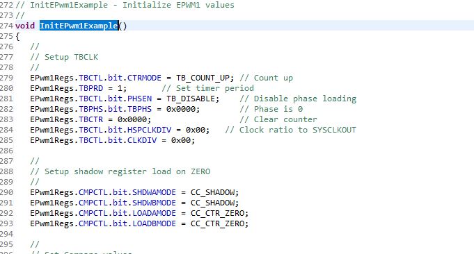
Clock settings I changed and code changes highlighted in the following images>


Above image is oscilloscope print connected on GPIO25 pin.
Let me know if my understanding and configurations are wrong.
Is this the maximum frequency we can obtain with this EPWM up counting?
Thanks,
Akshay


