


Other Parts Discussed in Thread: C2000WARE
Tool/software: Code Composer Studio
Hello all,
I am trying to implement sci echo back with CPU02 (by modifying the dual cpu blinky example). Now here are the steps that I am taking.
1) Handling the GPIO for sci to CPU02 from CPU01
GPIO_SetupPinMux(43, GPIO_MUX_CPU2, 0xF);
GPIO_SetupPinOptions(43, GPIO_INPUT, GPIO_PUSHPULL);
GPIO_SetupPinMux(42, GPIO_MUX_CPU2, 0xF);
GPIO_SetupPinOptions(42, GPIO_OUTPUT, GPIO_ASYNC);
2) Sending the data from Cpu02 to the sci data registers.
here is the cpu01 code-
//###########################################################################
//
// FILE: blinky_cpu01.c
//
// TITLE: LED Blink Example for F2837xD.
//
//! \addtogroup dual_example_list
//! <h1> Blinky </h1>
//!
//! Dual Core Blinky Example. This example demonstrates how to implement
//! and run a standalone application on both cores.
//!
//
//###########################################################################
// $TI Release: F2837xD Support Library v3.05.00.00 $
// $Release Date: Thu Oct 18 15:48:42 CDT 2018 $
// $Copyright:
// Copyright (C) 2013-2018 Texas Instruments Incorporated - http://www.ti.com/
//
// Redistribution and use in source and binary forms, with or without
// modification, are permitted provided that the following conditions
// are met:
//
// Redistributions of source code must retain the above copyright
// notice, this list of conditions and the following disclaimer.
//
// Redistributions in binary form must reproduce the above copyright
// notice, this list of conditions and the following disclaimer in the
// documentation and/or other materials provided with the
// distribution.
//
// Neither the name of Texas Instruments Incorporated nor the names of
// its contributors may be used to endorse or promote products derived
// from this software without specific prior written permission.
//
// THIS SOFTWARE IS PROVIDED BY THE COPYRIGHT HOLDERS AND CONTRIBUTORS
// "AS IS" AND ANY EXPRESS OR IMPLIED WARRANTIES, INCLUDING, BUT NOT
// LIMITED TO, THE IMPLIED WARRANTIES OF MERCHANTABILITY AND FITNESS FOR
// A PARTICULAR PURPOSE ARE DISCLAIMED. IN NO EVENT SHALL THE COPYRIGHT
// OWNER OR CONTRIBUTORS BE LIABLE FOR ANY DIRECT, INDIRECT, INCIDENTAL,
// SPECIAL, EXEMPLARY, OR CONSEQUENTIAL DAMAGES (INCLUDING, BUT NOT
// LIMITED TO, PROCUREMENT OF SUBSTITUTE GOODS OR SERVICES; LOSS OF USE,
// DATA, OR PROFITS; OR BUSINESS INTERRUPTION) HOWEVER CAUSED AND ON ANY
// THEORY OF LIABILITY, WHETHER IN CONTRACT, STRICT LIABILITY, OR TORT
// (INCLUDING NEGLIGENCE OR OTHERWISE) ARISING IN ANY WAY OUT OF THE USE
// OF THIS SOFTWARE, EVEN IF ADVISED OF THE POSSIBILITY OF SUCH DAMAGE.
// $
//###########################################################################
//
// Included Files
//
#include "F28x_Project.h"
#include "F2837xD_Ipc_drivers.h"
//
// Main
//
void main(void)
{
Uint16 i=0;
//
// Step 1. Initialize System Control:
// PLL, WatchDog, enable Peripheral Clocks
// This example function is found in the F2837xD_SysCtrl.c file.
//
InitSysCtrl();
#ifdef _STANDALONE
#ifdef _FLASH
//
// Send boot command to allow the CPU2 application to begin execution
//
IPCBootCPU2(C1C2_BROM_BOOTMODE_BOOT_FROM_FLASH);
#else
//
// Send boot command to allow the CPU2 application to begin execution
//
IPCBootCPU2(C1C2_BROM_BOOTMODE_BOOT_FROM_RAM);
#endif
#endif
//
// Call Flash Initialization to setup flash waitstates
// This function must reside in RAM
//
#ifdef _FLASH
InitFlash();
#endif
//
// Step 2. Initialize GPIO:
// This example function is found in the F2837xD_Gpio.c file and
// illustrates how to set the GPIO to it's default state.
//
InitGpio(); // Skipped for this example
EALLOW;
GpioCtrlRegs.GPADIR.bit.GPIO31 = 1;
GPIO_SetupPinMux(43, GPIO_MUX_CPU2, 0xF);
GPIO_SetupPinOptions(43, GPIO_INPUT, GPIO_PUSHPULL);
GPIO_SetupPinMux(42, GPIO_MUX_CPU2, 0xF);
GPIO_SetupPinOptions(42, GPIO_OUTPUT, GPIO_ASYNC);
for(i=0;i<8;i++)
{
GPIO_SetupPinMux(i,GPIO_MUX_CPU2,0);
GPIO_SetupPinOptions(i, GPIO_INPUT,GPIO_PULLUP);
}
//
// TODO Add code to allow configuration of GPADIR from CPU02 using IPC
//
EDIS;
GpioDataRegs.GPADAT.bit.GPIO31 = 1;// turn off LED
//
// Step 3. Clear all interrupts and initialize PIE vector table:
// Disable CPU interrupts
//
DINT;
//
// Initialize the PIE control registers to their default state.
// The default state is all PIE interrupts disabled and flags
// are cleared.
// This function is found in the F2837xD_PieCtrl.c file.
//
InitPieCtrl();
//
// Disable CPU interrupts and clear all CPU interrupt flags:
//
IER = 0x0000;
IFR = 0x0000;
//
// Initialize the PIE vector table with pointers to the shell Interrupt
// Service Routines (ISR).
// This will populate the entire table, even if the interrupt
// is not used in this example. This is useful for debug purposes.
// The shell ISR routines are found in F2837xD_DefaultIsr.c.
// This function is found in F2837xD_PieVect.c.
//
InitPieVectTable();
//
// Enable global Interrupts and higher priority real-time debug events:
//
EINT; // Enable Global interrupt INTM
ERTM; // Enable Global realtime interrupt DBGM
//
// Step 6. IDLE loop. Just sit and loop forever (optional):
//
for(;;)
{
//
// Turn on LED
//
GpioDataRegs.GPADAT.bit.GPIO31 = 0;
//
// Delay for a bit.
//
DELAY_US(1000 * 500);
//
// Turn off LED
//
GpioDataRegs.GPADAT.bit.GPIO31 = 1;
//
// Delay for a bit.
//
DELAY_US(1000 * 500);
}
}
//
// End of file
//
CPU02 code
//
// Included Files
//
#include "F28x_Project.h"
#include "F2837xD_Ipc_drivers.h"
Uint16 LoopCount;
//
// Function Prototypes
//
void scia_echoback_init(void);
void scia_fifo_init(void);
void scia_xmit(int a);
void scia_msg(char *msg);
void scia_xmit32(Uint32 b);
//
// Main
//
#ifdef _FLASH
//
// These are defined by the linker (see device linker command file)
//
extern Uint16 RamfuncsLoadStart;
extern Uint16 RamfuncsLoadSize;
extern Uint16 RamfuncsRunStart;
#endif
//
// Main
//
void main(void)
{
char *msg;
//
// Copy time critical code and Flash setup code to RAM
// This includes InitFlash(), Flash API functions and any functions that are
// assigned to ramfuncs section.
// The RamfuncsLoadStart, RamfuncsLoadEnd, and RamfuncsRunStart
// symbols are created by the linker. Refer to the device .cmd file.
//
#ifdef _FLASH
memcpy(&RamfuncsRunStart, &RamfuncsLoadStart, (size_t)&RamfuncsLoadSize);
#endif
//
// Step 1. Initialize System Control:
// PLL, WatchDog, enable Peripheral Clocks
// This example function is found in the F2837xD_SysCtrl.c file.
//
InitSysCtrl();
//
// Call Flash Initialization to setup flash waitstates
// This function must reside in RAM
//
#ifdef _FLASH
InitFlash();
#endif
//
// Step 2. Initialize GPIO:
// This example function is found in the F2837xD_Gpio.c file and
// illustrates how to set the GPIO to it's default state.
//
// InitGpio(); // Skipped for this example
EALLOW;
//
//TODO Add code to configure GPADIR through IPC
//
//GPIO_WritePin(34, 1);
//
// Step 3. Clear all interrupts and initialize PIE vector table:
// Disable CPU interrupts
//
DINT;
//
// Initialize the PIE control registers to their default state.
// The default state is all PIE interrupts disabled and flags
// are cleared.
// This function is found in the F2837xD_PieCtrl.c file.
//
InitPieCtrl();
//
// Disable CPU interrupts and clear all CPU interrupt flags:
//
IER = 0x0000;
IFR = 0x0000;
//
// Initialize the PIE vector table with pointers to the shell Interrupt
// Service Routines (ISR).
// This will populate the entire table, even if the interrupt
// is not used in this example. This is useful for debug purposes.
// The shell ISR routines are found in F2837xD_DefaultIsr.c.
// This function is found in F2837xD_PieVect.c.
//
InitPieVectTable();
//
// Enable global Interrupts and higher priority real-time debug events:
//
EINT; // Enable Global interrupt INTM
ERTM; // Enable Global realtime interrupt DBGM
//
// Step 6. IDLE loop. Just sit and loop forever (optional):
//
scia_fifo_init(); // Initialize the SCI FIFO
scia_echoback_init(); // Initialize SCI for echoback
msg = "\r\n\n\nHello World!\0";
scia_msg(msg);
msg = "\r\nYou will enter a character, and the DSP will echo it back! \n\0";
scia_msg(msg);
for(;;)
{
msg = "\r\nEnter a character: \0";
scia_msg(msg);
//
// Wait for inc character
//
/* while(SciaRegs.SCIFFRX.bit.RXFFST == 0) { } // wait for empty state
//
// Get character
//
ReceivedChar = SciaRegs.SCIRXBUF.all;
//
// Echo character back
//
msg = " You sent: \0";
scia_msg(msg);
scia_xmit(ReceivedChar);
LoopCount++;*/
scia_xmit32(GpioDataRegs.GPADAT.all);
DELAY_US(1000*500);
}
}
void scia_echoback_init()
{
//
// Note: Clocks were turned on to the SCIA peripheral
// in the InitSysCtrl() function
//
SciaRegs.SCICCR.all = 0x0007; // 1 stop bit, No loopback
// No parity,8 char bits,
// async mode, idle-line protocol
SciaRegs.SCICTL1.all = 0x0003; // enable TX, RX, internal SCICLK,
// Disable RX ERR, SLEEP, TXWAKE
SciaRegs.SCICTL2.all = 0x0003;
SciaRegs.SCICTL2.bit.TXINTENA = 1;
SciaRegs.SCICTL2.bit.RXBKINTENA = 1;
//
// SCIA at 9600 baud
// @LSPCLK = 50 MHz (200 MHz SYSCLK) HBAUD = 0x02 and LBAUD = 0x8B.
// @LSPCLK = 30 MHz (120 MHz SYSCLK) HBAUD = 0x01 and LBAUD = 0x86.
//
SciaRegs.SCIHBAUD.all = 0x0002;
SciaRegs.SCILBAUD.all = 0x008B;
SciaRegs.SCICTL1.all = 0x0023; // Relinquish SCI from Reset
}
//
// scia_xmit - Transmit a character from the SCI
//
void scia_xmit(int a)
{
while (SciaRegs.SCIFFTX.bit.TXFFST != 0) {}
SciaRegs.SCITXBUF.all =a;
}
// Function for transmitting 32bit integers because the SCITXBUF is least significant
//8 bit buffer
void scia_xmit32(Uint32 b)
{
int msg8bit,j;
for( j=0;j<8;j++)
{
msg8bit=((b>>j)&1)+48;
while (SciaRegs.SCIFFTX.bit.TXFFST != 0) {}
SciaRegs.SCITXBUF.all =msg8bit;
}
}
//
// scia_msg - Transmit message via SCIA
//
void scia_msg(char * msg)
{
int i;
i = 0;
while(msg[i] != '\0')
{
scia_xmit(msg[i]);
i++;
}
}
//
// scia_fifo_init - Initialize the SCI FIFO
//
void scia_fifo_init()
{
SciaRegs.SCIFFTX.all = 0xE040;
SciaRegs.SCIFFRX.all = 0x2044;
SciaRegs.SCIFFCT.all = 0x0;
}
//
// End of file
//
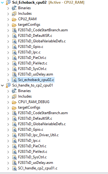
here is the snapshot of project folder and added files-
It seems like the CPU02 is not getting access to the SCI registers.
Please help.
Thanks in advance.

