Dear Champs,
I am asking this for our customer.
In the user's application, they need to alternate the voltage and then get the corresponding current.
Now, they found an issue and we wonder if this is related to the ADC channel-to-channel errors.
Their setting is as follows:
SOC0 ADCINA4 ACQPS=8
SOC1 ADCINA3 ACQPS=8
SOC2 ADCINA6 ACQPS=8
SOC3 ADCINA7 ACQPS=8
All of the above use the same PWM triggering source with round robin setting.
ADCNONOVERLAP is set.
ADCCLK = 30 MHz
F28027 rev. A is used.
The user was trying to input alternating 0 and 3.3V in A6 and found that A7 reading was changing with the change of A6 from 0 to 3.3V and from 3.3V to 0. Note that the A7 channel was stable on the oscilloscope, but they output the A7 ADC readings to another PWM with Low-pass as DAC to observe it on the oscilloscope.
Note that in the testing, DC supply was used to input to A6 and A7 directly without any series resistors so that the ADC source impedance is very small.
By observation,
This A7 reading changing with A6 input would become larger when A7 DC input is larger.
If both ACQPS of A6 (SOC2) and A7 (SOC3) were increased by a lot, then the A7 reading changing with A6 input would be no more.
If they did not alternate A6 input, then A7 reading would not be changing, either.
From the above, our questions:
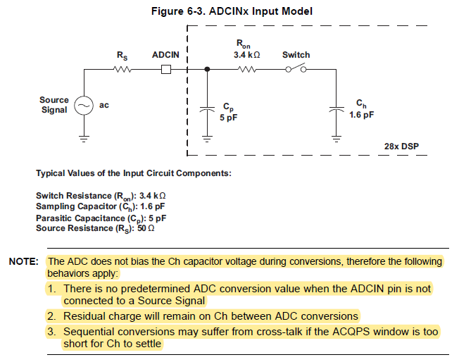
Q1: Is this A7 reading changing with A6 input just the channel-to-channel gain variation (+-4LSB) and channel-to-channel offset variation (+-4LSB) documented in Talbe 6-26 (P76) of the datasheet (http://www.ti.com/lit/ds/symlink/tms320f28027.pdf)? Is this so-called cross-talk?
Q2: Why are there such channel-to-channel gain/offset variation?
Q3: After A6 is sampled by the internal sampling cap (Ch) and then changed to A7 by the multiplexer, the Ch will be charged from zero or from the last value of A6? We wonder if this explains why A6 affects A7 in this case?
Q4: To avoid such error, can they just change the SOC order so that A6 is in the last? like
SOC0 ADCINA4 ACQPS=8
SOC1 ADCINA3 ACQPS=8
SOC2 ADCINA7 ACQPS=8
SOC3 ADCINA6 ACQPS=8
Q5: With newer devices like F280049, which has up to 3x ADC modules and 3x S/H. If ADC A6 is allocated on ADC A, then all the ADC A signals measured after A6 will be affected, but other signals measured on ADC B and ADC C will not be affected. Is our understanding correct?
Wayne Huang