This thread has been locked.

If you have a related question, please click the "Ask a related question" button in the top right corner. The newly created question will be automatically linked to this question.

TMS320F28377S: Pins related to internal ADC

Part Number: TMS320F28377S

I have 2 questions related to internal ADC.

Q1. This question is for biasing at VREFHIA to VREFHID pins.

     Is it work well to bias the pins by 3V power source directly as AVDDREFBG pin of F2812?

    P.1464 and P.1465 of the technical reference of F28377S, spruhx5g.pdf describes
     that those pins are biased by buffered reference voltage,
     but. I want to reduce the external reference ICs and buffers, if possible.
     This is the background of this question.

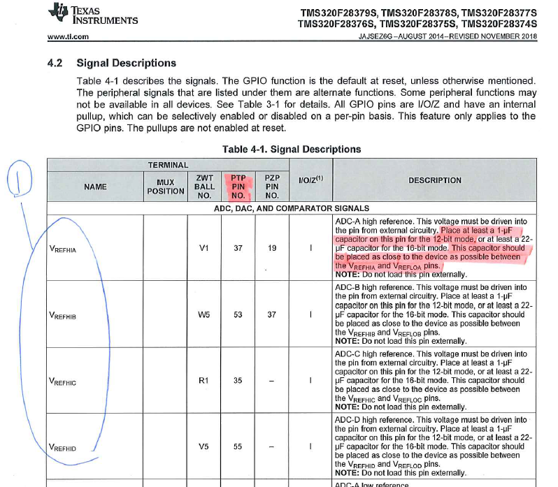
     I also referred the following table in P.17 of datasheet.  This is just information.
   [cid:image001.png@01D5CBCA.D2014AB0]

Q2. This question is for ADC input pins.

Some of ADCINxx pins, which are marked in the following table in page.17
and 18 of datasheet, has 50kohm pull-down or 100pF cap.  PLS also refer
the following table.
How should the effect by the internal resistor and the cap be estimated related with ADC input pin without such internal constant?

What is the reason why the internal constants are added?

[cid:image002.png@01D5CBCC.41418EC0]

Best Regards,

  • Hi Naoki,

    The ADC and ADC reference on this device is different from that on the F2812.  You will need to build some circuit to drive a low-noise reference voltage into the reference pins.  We have some recommended circuits in the TRM section "Designing an External Reference Circuit".

    These components are parasitic value based on what else is muxed on the pin. 

    The capacitor is there due to the DAC optional reference voltage being muxed on that pin; additional capacitance is needed to internally stabilize the reference voltage.  This one will likely just result in a slightly longer S+H time when you go to calculate the expected settling time.  Alternately, you can make the settling time pretty similar to other inputs if you reduce the capacitance on the pin. e.g. if you calculate that you need a 270pF capacitor on the ADC pin you might only put ~170pF on the pin muxed with VDAC.

    The resistors are there because the buffered DAC output is muxed with the ADC input.  For these you can compensate by using a lower impedance driver and/or selecting a lower-priority signal that can tolerate a little bit of DC error due to the voltage divider formed by the resistance of your source and the parasitic resistance.