This thread has been locked.

If you have a related question, please click the "Ask a related question" button in the top right corner. The newly created question will be automatically linked to this question.

CCS/LAUNCHXL-F28379D: Same Adc Bases Creating Noise to Each Other

Part Number: LAUNCHXL-F28379D
Other Parts Discussed in Thread: TMS320F28379D, C2000WARE

Tool/software: Code Composer Studio

Hello there
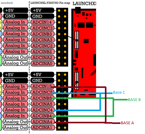
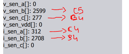
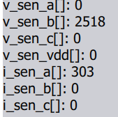
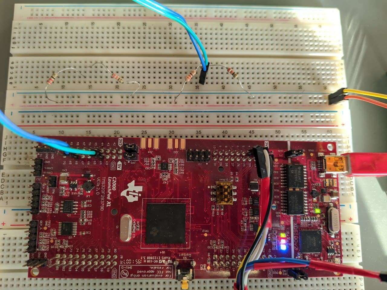
I use LAUNCHXL-F28379D launchpad. I have to do 6 ACD readings in my application. But the adc pins on the same base make noise to each other. When I connect a potentiometer to ADCINB5, one of the pins I specified in the picture for the test, it affects ADCINB4 and creates noise. This is the same for BASEA and BASEC. When I connect an adc sensor to one pin, it affects the other. What is the reason for this and is there a solution?

  • Hi '8118,

    Do you buffer the signal at the potentiometer output?  If not, what is the effective impedance of the potentiometer?  What S+H duration are you using (set by the ACQPS setting of the SOC configuration)?    

    Are the signals that are affecting each other sampled sequentially?  You may want to have a look at the description of "Memory Cross-Talk" in the following application note: 

    https://www.ti.com/lit/an/spract6/spract6.pdf


  • I am facing the same problem. I adapted it to my code by following the application note you suggested, but there was no change. When I sent the data to my computer via SCI, I got the following results.

    This is the result when I remove the input to the ADC INB4 pin for a better understanding.

  • Hi M.D.

    What is the actual voltage source? What is the sampling order for your example above?  What is the input impedance?  What was the selected S+H duration?  Are the multiple ADCs triggered by the same trigger? 

  • Hi Devin,

    I am using the TMS320F28379D Launchpad. I supply the device through the USB port. I send a constant voltage to the ADC channels through a voltage divider circuit. I have externally supplied a constant voltage to the voltage divider circuit.

    I was using the voltage and ground outputs of the device before feeding the voltage divider circuit externally. I got the same results when I made such a supply.The voltage was 3.3 V. The reason I changed the source is that I came across such a document regarding cross-talk.

    https://www.maximintegrated.com/en/design/technical-documents/app-notes/1/1761.html

    The sampling order in my code is as follows:

    It tells us not to use single or double channels consecutively in the document you suggested. I applied it as stated in the document:

    In addition, while investigating this situation, I encountered a situation like this in erratashet:

    But this error is only degraded to channel A, for my situation, I have encountered with same problems on other chanelles, ie. A, B,C Channels. Now, I am investigating reason of this problem in the reference manuel. 

    I don't know the input impedance, but I referenced the reference manual for the sampling time.I also took this event as a reference and checked the minimum time required from the datasheet.

    CCS/TMS320F280025C: How to set the ACQPS (sample window ) for an ADC. - C2000 microcontrollers forum...

    e2e.ti.com
    Part Number: TMS320F280025C Tool/software: Code Composer Studio Hi, I am working on internal ADC and using 3.3V Internal reference. I am unable to get closer

    I set the ADC clock value to 50 Mhz. Since the system clock of my device is 200 Mhz, then divider value is four.I increased the acquisition window up to 4 times on average, but the result remained unchanged.

  • Hi M.D,

    Using a voltage divider from the supplies is going to cause 2 issues:

    • Input impedance is high (it'll be the parallel combination of the two resistors in your divider)
    • Supplies are noisy

    You'll also need to add some sort of capacitance to the ADC input.  Nominally this would be about 20 x Ch (about 290 pF), but if you are sampling slow you can get away with using a large capacitor to do "charge sharing" which is closer to Ch * 4096 * 2 (about 120nF).  Charge-sharing will allow use of a short S+H time and will possibly provide some noise filtering.    

    In either case, you should use the TINA models in the linked app. note to simulate input settling over multiple cycles to determine an appropriate sample rate (charge sharing) or S+H duration (regular ADC input drive method).  

    Your input is also going to be pretty noisy from the breadboard traces, through-hole component leads, and the floating wires. Overall I'd recommend that you highly average the results to start out to ensure the DC level is being read correctly, then work on cleaning up the various noise sources.

    ---

    I'm not sure what you mean by "It tells us not to use single or double channels consecutively". There is no restriction or recommendation against any particular sequence of channel sampling. The section you quoted describes what type of errors you will likely see if (and only if) the input settling design is not correct. 

    ---

    This erratum is unlikely to apply to your device, as it only applies to device revisions 0 and A, while production released devices are on revision C. It is maybe possible that you have revision A silicon if you have a very old launchpad.  You can use the device errata to determine how to read the markings on the device, or you can read the REVID register on the device.    

    ---   

    The minimum S+H duration is only going to be applicable if you are using a high-BW op-amp with a low series R to drive the ADC input (or using charge-sharing input design).  See the previously linked app. note for the comprehensive guide to selecting the S+H duration using SPICE simulation, or you can get a good estimate using the formula in the "choosing an acquisition window duration" section of the device TRM   

    Note that if the effective input impedance of the resistive voltage divider is too high, it is possible that not even the max ACQPS setting (511) will give good settling.  This is 512*5ns =  2.56us, which is more than 30x the minimum S+H duration.  

    ---

    As designed, your SW triggering method will result in asynchronous operation between the ADCs (see "ensuring synchronous operation" section of the TRM).  This has some performance impactions for the ADC (see "ADC-to-ADC Isolation" and "ENOB" specifications in the datasheet).  

    If you intend to SW trigger your ADC results, you should follow the parallel SW trigger example in c2000ware to ensure all your ADCs start converting simultaneously.  Otherwise, using the ePWM to trigger the results should also prevent this issue.