This thread has been locked.
If you have a related question, please click the "Ask a related question" button in the top right corner. The newly created question will be automatically linked to this question.
Hi,
[Question1]
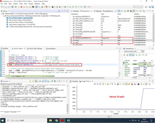
I use an internal temperature sensor to monitor the temperature, but sometimes it captures abnormal values.
Looking at the errata, it says to lengthen the sampling period from the error "ADC: Temperature Sensor Minimum Sample Window Requirement".
I increased ACQPS from 6 to 63, but the situation doesn't improve.
Please let me know if you have any countermeasures.
[Question2]
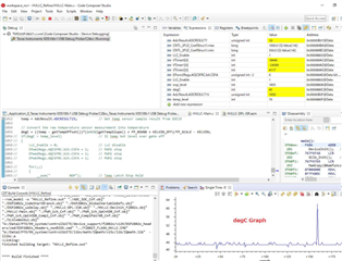
Does the error "ADC: Initial Conversion" described in Errata (sprz292s) of TMS320F2802x exist even on the devices currently on the market?
Thanks,
Koki
Hello,
A subject-matter expert reply your question. However, we have been dealing with inclement weather and power outages in the area and responses may be slow.
Koki,
Yes, this errata applies to devices currently in production.
If you are only sampling the internal temperature sensor with the ADC you will need to perform a dummy sample on this input to avoid the ADC first sample issue. In this case there is no need to shorten the sample and hold window of the temp sensor sample as this meets the other workaround listed for the temp sensor min sample case.
Let me know if this addresses your issue, or you still see abnormalities with the workaround in place.
Best,
Matthew
Koki,
For the purpose of debug could you try the workaround #1 and see if it resolves the issue you see? #2 will work, but there are also restrictions on the valid values for ACQPS listed in the TRM. I'd like to make sure we can get good results from #1 and then we can get the right ACQPS to make #2 work.
Best,
Matthew
Hi, Matthew
> there are also restrictions on the valid values for ACQPS listed in the TRM.
I couldn't find a description in TRM about the limits of ACQPS. Where on what page is it listed?
I have already verified # 1.
It is incorporated into SOC14 and SOC15 for double-sampling. Both may be abnormal.
# 2 I increased ACQPS from 6 to 63, but the value doesn't improve.
Currently, abnormal output is avoided by detecting when the reference temperature is exceeded 10 times in a row.
Please let me know if you have any countermeasures.
Best,
Koki
Koki,
Would you be able to post 10 consecutive values from the temp sensor for just SOC15(discard SOC14), for me to see the magnitude of the difference. If its simpler you could make all conversions SOC0-15 read the temp sensor (and then trigger them all) and report out SOC1-15.
If you could also attach the C file where you've set up the ADC I can take a look at that as well.
Can you also comment on the resolution in degrees C that you are trying to use in your system? i.e. you need to detect a 10 deg rise/fall, etc.
Best,
Matthew
Matthew
I'm sorry for being late.
>Would you be able to post 10 consecutive values from the temp sensor for just SOC15(discard SOC14),
Since the value of the anomaly is rare, I attach the graph of CCS instead of the conversion result of 10 consecutive pieces.
■Nomal value
AdcResult.ADCRESULT15(=temp) = 1914~1921
degC=40~42
■Abnormal value
AdcResult.ADCRESULT15(=temp) = 4090
degC=429
■temp graph
If an abnormal temperature is detected, the operation will stop.
Therefore, the image remains anomalous value, but the anomalous value occurs temporarily.
■ degC graph
>If you could also attach the C file where you've set up the ADC I can take a look at that as well.
Attach the main.c file that sets up the ADC.
//---------------------------------------------------------------------------------- // FILE: HVLLC-Main.C <Refine> // // Description: Half-Bridge LLC Resonant DC/DC Converter with Synchronous Rectification // // Version: 1.0 // // Target: TMS320F2802x (PiccoloA), // //---------------------------------------------------------------------------------- // Copyright Texas Instruments 2004-2010 //---------------------------------------------------------------------------------- // Revision History: //---------------------------------------------------------------------------------- // Date | Description / Status //---------------------------------------------------------------------------------- // 2011.05.15 First edition // 2020.10.23 REMORT ON/OFF // 2020.10.28 OVP // 2020.11.04 Temp // 2020.12.16 Soft Start // 2020.12.18 Voltage monitoring //---------------------------------------------------------------------------------- // // PLEASE READ - Useful notes about this Project // Although this project is made up of several files, the most important ones are: // "HVLLC-Main.C" - this file // - Application Initialization, Peripheral config, // - Application management // - Slower background code loops and Task scheduling // "HVLLC-DevInit_F28xxx.C // - Device Initialization, e.g. Clock, PLL, WD, GPIO mapping // - Peripheral clock enables // - DevInit file will differ per each F28xxx device series, e.g. F280x, F2833x, // "HVLLC-DPL-ISR.asm // - Assembly level library Macros and any cycle critical functions are found here // "HVLLC-Settings.h" // - Global defines (settings) project selections are found here // - This file is referenced by both C and ASM files. // // Code is made up of sections, e.g. "FUNCTION PROTOTYPES", "VARIABLE DECLARATIONS" ,..etc // each section has FRAMEWORK and USER areas. // FRAMEWORK areas provide useful ready made "infrastructure" code which for the most part // does not need modification, e.g. Task scheduling, ISR call, GUI interface support,...etc // USER areas have functional example code which can be modified by USER to fit their appl. // // Code can be compiled with various build options (Incremental Builds IBx), these // options are selected in file "HVLLC-Settings.h". Note: "Rebuild All" compile // tool bar button must be used if this file is modified. //---------------------------------------------------------------------------------- #include "PeripheralHeaderIncludes.h" #include "DSP2802x_EPWM_defines.h" #include "HVLLC-Settings.h" #include "DPlib.h" #include "IQmathLib.h" #include <math.h> //%%%%%%%%%%%%%%%%%%%%%%%%%%%%%%%%%%%%%%%%%%%%%%%%%%%%%%%%%%%%%%%%%%%%%%%%%%%%%%%%%% // FUNCTION PROTOTYPES //%%%%%%%%%%%%%%%%%%%%%%%%%%%%%%%%%%%%%%%%%%%%%%%%%%%%%%%%%%%%%%%%%%%%%%%%%%%%%%%%%% // Add protoypes of functions being used in the project here extern interrupt void CNTL_ISR(void); extern interrupt void PWM_ISR(void); void DeviceInit(void); #ifdef FLASH void InitFlash(); #endif void MemCopy(); void SCIA_Init(); void SerialHostComms(); //-------------------------------- DPLIB -------------------------------------------- void PWM_ComplPairDB_CNF(int16 n, int16 period, int16 mode, int16 phase); void PWM_ComplPairDB_UpdateDB(int16 n, int16 dbRED, int16 dbFED); void PWM_1ch_UpCntDB_CNF(int16 n, int16 period, int16 mode, int16 phase); void PWM_1ch_UpCntDB_UpdateDB(int16 n, int16 dbRED, int16 dbFED); void PWM_1ch_UpCntDB_Compl_CNF(int16 n, int16 period, int16 mode, int16 phase); void PWM_1ch_UpCntDB_Compl_UpdateDB(int16 n, int16 dbRED, int16 dbFED); void PWM_1ch_CNF(int16 n, int16 period, int16 mode, int16 phase); void ADC_SOC_CNF(int ChSel[], int TrigSel[], int ACQPS[], int IntChSel, int mode); // -------------------------------- FRAMEWORK -------------------------------------- // State Machine function prototypes //---------------------------------------------------------------------------------- // Alpha states void A0(void); //state A0 void B0(void); //state B0 void C0(void); //state C0 // A branch states void A1(void); //state A1 void A2(void); //state A2 // B branch states void B1(void); //state B1 void B2(void); //state B2 // C branch states void C1(void); //state C1 // Variable declarations void (*Alpha_State_Ptr)(void); // Base States pointer void (*A_Task_Ptr)(void); // State pointer A branch void (*B_Task_Ptr)(void); // State pointer B branch void (*C_Task_Ptr)(void); // State pointer C branch //---------------------------------------------------------------------------------- //%%%%%%%%%%%%%%%%%%%%%%%%%%%%%%%%%%%%%%%%%%%%%%%%%%%%%%%%%%%%%%%%%%%%%%%%%%%%%%%%%% // VARIABLE DECLARATIONS - GENERAL //%%%%%%%%%%%%%%%%%%%%%%%%%%%%%%%%%%%%%%%%%%%%%%%%%%%%%%%%%%%%%%%%%%%%%%%%%%%%%%%%%% // -------------------------------- FRAMEWORK -------------------------------------- #define numTimers 1 int16 VTimer0[numTimers]; // Virtual Timers slaved off CPU Timer 0 int16 VTimer1[numTimers]; // Virtual Timers slaved off CPU Timer 1 int16 VTimer2[numTimers]; // Virtual Timers slaved off CPU Timer 2 int16 SerialCommsTimer; int16 CommsOKflg; // Used for running BackGround in flash, and ISR in RAM extern Uint16 *RamfuncsLoadStart, *RamfuncsLoadEnd, *RamfuncsRunStart; // Used for ADC Configuration int ChSel[16]; // = {0,0,0,0,0,0,0,0,0,0,0,0,0,0,0,0}; int TrigSel[16]; // = {0,0,0,0,0,0,0,0,0,0,0,0,0,0,0,0}; int ACQPS[16]; // = {6,6,6,6,6,6,6,6,6,6,6,6,6,6,6,6}; // ---------------------------------- USER ----------------------------------------- int16 LLC_Enable; // 1 = Enable, 0 = Disable int16 SR_Enable; // 1 = Enable, 0 = Disable int16 Comp_Enable; // 1 = Enable, 0 = Disable int16 Pgain; // PID P gain (Q10) int16 Igain; // PID I gain (Q10) int16 Dgain; // PID D gain (Q10) int16 use_2P2Z; // use 2P2Z coefficients instead of PID int16 update_coeffs; // flag used to trigger update of 2P2Z coefficients long b2_coeff; long b1_coeff; long b0_coeff; long a2_coeff; long a1_coeff; // 2020.10.28 OVP int16 ovp_level; // OVP LEVEL // 2020.11.4 Temp int16 temp; // raw temperature sensor reading int16 degC; // temperature in deg. C int16 OFFSET; // temperature OFFSET int16 SLOPE; // temperature SLOPE int16 temp_level; // temperature OFF level int16 temp_count; // temperature count // 2020.12.16 Soft Start int16 ss_kaisi; // Soft Start flag int16 ss_first; // Soft Start first time long ss_inc; // Soft Start period increment // 2020.12.18 Voltage monitoring int16 Vcc_on; // C2000 piccolo DSP Vcc Voltage int16 Vsen1; // DCDC input Voltage signal 1 int16 Vsen2; // DCDC input Voltage signal 2 // ---------------------------- DPLIB Net Pointers --------------------------------- // Declare net pointers that are used to connect the DP Lib Macros here // ADC extern volatile long *ADCDRV_1ch_Rlt7; // Vout // 2P2Z extern volatile long *CNTL_2P2Z_Ref1; extern volatile long *CNTL_2P2Z_Fdbk1; extern volatile long *CNTL_2P2Z_Out1; extern volatile long *CNTL_2P2Z_Coef1; // PWM extern volatile long *PWMDRV_LLC_ComplPairDB_Duty1; extern volatile long *PWMDRV_LLC_ComplPairDB_Period1; extern volatile long *PWMDRV_LLC_1ch_UpCntDB_Compl_Duty2; extern volatile long *PWMDRV_LLC_1ch_UpCntDB_Compl_Period2; extern volatile long *PWMDRV_LLC_1ch_UpCntDB_Duty3; extern volatile long *PWMDRV_LLC_1ch_UpCntDB_Period3; // ---------------------------- DPLIB Variables --------------------------------- // Declare the net variables being used by the DP Lib Macro here volatile long Vout; volatile long Duty1; volatile long Duty2; volatile long Duty3; volatile long Period; long Vset; // Control loop target long Min_Period; // Minimum PWM period long Max_Period; // Maximum PWM period int16 RED; // Half-Bridge PWM1 Rising Edge Delay int16 FED; // Half-Bridge PWM1 Falling Edge Delay int16 REM1; // SR1 PWM2 Rising Edge Margin int16 FEM1; // SR1 PWM2 Falling Edge Margin int16 REM2; // SR2 PWM3 Rising Edge Margin int16 FEM2; // SR2 PWM3 Falling Edge Margin int16 COMP1; // SR1 Comparator Trip Value int16 COMP2; // SR2 Comparator Trip Value #pragma DATA_SECTION(CNTL_2P2Z_CoefStruct1, "CNTL_2P2Z_Coef"); struct CNTL_2P2Z_CoefStruct CNTL_2P2Z_CoefStruct1; //%%%%%%%%%%%%%%%%%%%%%%%%%%%%%%%%%%%%%%%%%%%%%%%%%%%%%%%%%%%%%%%%%%%%%%%%%%%%%%%%%% // VARIABLE DECLARATIONS - CCS WatchWindow / GUI support //%%%%%%%%%%%%%%%%%%%%%%%%%%%%%%%%%%%%%%%%%%%%%%%%%%%%%%%%%%%%%%%%%%%%%%%%%%%%%%%%%% // -------------------------------- FRAMEWORK -------------------------------------- //GUI support variables // sets a limit on the amount of external GUI controls - increase as necessary int16 *varSetTxtList[16]; //16 textbox controlled variables int16 *varSetBtnList[16]; //16 button controlled variables int16 *varSetSldrList[16]; //16 slider controlled variables int16 *varGetList[16]; //16 variables sendable to GUI int16 *arrayGetList[16]; //16 arrays sendable to GUI int16 LedBlinkCnt; // ---------------------------------- USER ----------------------------------------- int16 FlashID; // Monitor ("Get") // Display as: int16 Gui_Vout; // Q9 int16 Gui_Ipri; // Q9 int16 Gui_V_SR1; // Q9 int16 Gui_V_SR2; // Q9 int16 Gui_I_SR1; // Q8 int16 Gui_I_SR2; // Q8 // Configure ("Set") int16 Gui_Vset; // Q9 // History arrays are used for Running Average calculation (boxcar filter) // Used for CCS display and GUI only, not part of control loop processing Uint16 Hist_Vout[HistorySize]; Uint16 Hist_Ipri[HistorySize]; Uint16 Hist_V_SR1[HistorySize]; Uint16 Hist_V_SR2[HistorySize]; Uint16 Hist_I_SR1[HistorySize]; Uint16 Hist_I_SR2[HistorySize]; //Scaling Constants (values found via spreadsheet; exact value calibrated per board) Uint16 K_Vout; // Uint16 K_Ipri; // Uint16 K_V_SR1; // Uint16 K_V_SR2; // Uint16 K_I_SR1; // Uint16 K_I_SR2; // Uint16 iK_Vset; // // Variables for background support only (no need to access) int16 i; // common use incrementer Uint32 HistPtr, temp_Scratch; // Temp here means Temporary //%%%%%%%%%%%%%%%%%%%%%%%%%%%%%%%%%%%%%%%%%%%%%%%%%%%%%%%%%%%%%%%%%%%%%%%%%%%%%%%%%% // MAIN CODE - starts here //%%%%%%%%%%%%%%%%%%%%%%%%%%%%%%%%%%%%%%%%%%%%%%%%%%%%%%%%%%%%%%%%%%%%%%%%%%%%%%%%%% void main(void) { //================================================================================= // INITIALISATION - General //================================================================================= // The DeviceInit() configures the clocks and pin mux registers // The function is declared in HVLLC-DevInit_F2803/2x.c, // Please ensure/edit that all the desired components pin muxes // are configured properly that clocks for the peripherals used // are enabled, for example the individual PWM clock must be enabled // along with the Time Base Clock DeviceInit(); // Device Life support & GPIO SCIA_Init(); // Initalize the Serial Comms A peripheral //-------------------------------- FRAMEWORK -------------------------------------- // Only used if running from FLASH // Note that the variable FLASH is defined by the compiler with -d FLASH #ifdef FLASH // Copy time critical code and Flash setup code to RAM // The RamfuncsLoadStart, RamfuncsLoadEnd, and RamfuncsRunStart // symbols are created by the linker. Refer to the linker files. MemCopy(&RamfuncsLoadStart, &RamfuncsLoadEnd, &RamfuncsRunStart); // Call Flash Initialization to setup flash waitstates // This function must reside in RAM InitFlash(); // Call the flash wrapper init function #endif //(FLASH) // Timing sync for background loops // Timer period definitions found in PeripheralHeaderIncludes.h CpuTimer0Regs.PRD.all = mSec1; // A tasks CpuTimer1Regs.PRD.all = mSec10; // B tasks CpuTimer2Regs.PRD.all = mSec100; // C tasks // Tasks State-machine init Alpha_State_Ptr = &A0; A_Task_Ptr = &A1; B_Task_Ptr = &B1; C_Task_Ptr = &C1; for (i=0; i<numTimers; i++) { VTimer0[i] = 0; VTimer1[i] = 0; VTimer2[i] = 0; } SerialCommsTimer = 0; CommsOKflg = 0; LedBlinkCnt = 5; for (i=0; i<16; i++) { ChSel[i] = 0; TrigSel[i] = 0; ACQPS[i] = 6; } for(i=0; i<HistorySize; i++) { Hist_Vout[i] = 0; } // ---------------------------------- USER ----------------------------------------- // put common initialization/variable definitions here Pgain = 200; // Q10 Igain = 1; // Q10 Dgain = 5; // Q10 use_2P2Z = 1; // 2021.3.17 2P2Z use update_coeffs = 1; // 2021.3.17 2P2Z use b2_coeff = _IQ26(0.35); b1_coeff = _IQ26(-1.45); b0_coeff = _IQ26(1.33); a2_coeff = _IQ26(-0.23); a1_coeff = _IQ26(1.23); K_Vout = 19439; // 0.593 (Q15) K_Ipri = 19439; // 0.593 (Q15) K_V_SR1 = 19439; // 0.593 (Q15) K_V_SR2 = 19439; // 0.593 (Q15) K_I_SR1 = 16896; // 0.516 (Q15) K_I_SR2 = 16896; // 0.516 (Q15) iK_Vset = 27618; // 1.686 (Q14) Gui_Vset = 0; Vset = 5365000; // 2021.3.12 Vout=12V Adjustment (Q24) Duty1 = _IQ24(0.5); Duty2 = _IQ24(0.5); Duty3 = _IQ24(0.5); Period = _IQ14(550); Min_Period = _IQ14(MIN_PERIOD); Max_Period = _IQ14(MAX_PERIOD); RED = RisingEdgeDelay; FED = FallingEdgeDelay; REM1 = RisingEdgeMargin1; FEM1 = FallingEdgeMargin1; REM2 = RisingEdgeMargin2; FEM2 = FallingEdgeMargin2; COMP1 = CompTripLevel1; COMP2 = CompTripLevel2; LLC_Enable = DEMO_MODE; SR_Enable = 1; // 2021.3.12 SR enable GUI display only use Comp_Enable = 0; CNTL_2P2Z_CoefStruct1.b2 = _IQ16(Dgain); CNTL_2P2Z_CoefStruct1.b1 = _IQ16(Igain - Pgain - Dgain - Dgain); CNTL_2P2Z_CoefStruct1.b0 = _IQ16(Pgain + Igain + Dgain); CNTL_2P2Z_CoefStruct1.a2 = _IQ26(0.0); CNTL_2P2Z_CoefStruct1.a1 = _IQ26(1.0); CNTL_2P2Z_CoefStruct1.max = Max_Period; CNTL_2P2Z_CoefStruct1.min = Min_Period; // 2020.10.28 OVP ovp_level= 1835; // OVP_LEVEL�@=Vovp*Gfb*Gadc*= 17 * 0.087 *1241 = 1835 // Vovp�@���@17V Gfb=R18/�iR16+R18)�@��0.087 // Gadc=Gadc=2^(ADC res) / VfsvADC= 2^(12) /3.3= 1241 // reference HVLLC-Calculations.xls // 2020.11.4 Temp FlashRegs.FOTPWAIT.bit.OTPWAIT =1; #define FP_SCALE 32768 #define FP_ROUND FP_SCALE / 2 #define KELVIN 273 #define KELVIN_OFF FP_SCALE * KELVIN #define getTempSlope() (*(int(*)(void))0x3D7E80)() #define getTempOffset() (*(int(*)(void))0x3D7E83)() OFFSET = getTempOffset(); // For CCS expression window display SLOPE = getTempSlope(); // For CCS expression window display temp_level = 120; // temperature OFF level 120 deg. C temp_count = 0; // temperature count reset // 2020.12.16 Soft Start ss_kaisi = 0; // Soft Start flag ss_first = 0; // Soft Start first time ss_inc = _IQ14(SS_INC); // Soft Start period increment // 2020.12.18 Voltage monitoring Vcc_on = 3723; // C2000 piccolo DSP Vcc Voltage = 3.0V 4095/3.3V*3.0V=3723 Vsen1 = 0; // Vsen signal 1 reset Vsen2 = 0; // Vsen signal 2 reset //=============================================================================== // INITIALISATION - GUI connections //================================================================================= // Use this section only if you plan to "Instrument" your application using the // Microsoft C# freeware GUI Template provided by TI FlashID = FLASHID; //"Set" variables //--------------------------------------- // assign GUI variable Textboxes to desired "setable" parameter addresses varSetTxtList[0] = &Pgain; varSetTxtList[1] = &Igain; varSetTxtList[2] = &Dgain; varSetTxtList[3] = &RED; varSetTxtList[4] = &FED; varSetTxtList[5] = &REM1; varSetTxtList[6] = &FEM1; varSetTxtList[7] = &REM2; varSetTxtList[8] = &FEM2; varSetTxtList[9] = &COMP1; varSetTxtList[10] = &COMP2; // assign GUI Buttons to desired flag addresses varSetBtnList[0] = &LLC_Enable; varSetBtnList[1] = &SR_Enable; varSetBtnList[2] = &Comp_Enable; // assign GUI Sliders to desired "setable" parameter addresses varSetSldrList[0] = &Gui_Vset; //"Get" variables //--------------------------------------- // assign a GUI "getable" parameter address varGetList[0] = &FlashID; varGetList[1] = &Gui_Vout; varGetList[2] = &Gui_I_SR1; varGetList[3] = &Gui_I_SR2; // assign a GUI "getable" parameter array address // arrayGetList[0] = &DBUFF1; //only need to set initial position of array, // arrayGetList[1] = &DBUFF2; // program will run through it accordingly //================================================================================== // INCREMENTAL BUILD OPTIONS - NOTE: selected via HVLLC-Settings.h //================================================================================== // ---------------------------------- USER ----------------------------------------- #define IpriR AdcResult.ADCRESULT1 //Q12 #define V_SR1R AdcResult.ADCRESULT3 //Q12 #define V_SR2R AdcResult.ADCRESULT5 //Q12 #define I_SR1R AdcResult.ADCRESULT3 //Q12 #define I_SR2R AdcResult.ADCRESULT5 //Q12 #define VoutR AdcResult.ADCRESULT7 //Q12 #define Vcc AdcResult.ADCRESULT9 // 2020.12.18 C2000 piccolo DSP Vcc Voltage EPwm1Regs.AQCSFRC.bit.CSFA = 1; // EPWM1 OFF EPwm2Regs.AQCSFRC.bit.CSFA = 1; // EPWM2 OFF EPwm3Regs.AQCSFRC.bit.CSFA = 1; // EPWM3 OFF // Configure PWM1AB PWM_ComplPairDB_CNF(1, MIN_PERIOD, 1, 0); PWM_ComplPairDB_UpdateDB(1, RED, FED); // Configure PWM2A PWM_1ch_UpCntDB_Compl_CNF(2, MIN_PERIOD, 0, 0); PWM_1ch_UpCntDB_Compl_UpdateDB(2, REM1, FEM1); // Configure PWM3A PWM_1ch_UpCntDB_CNF(3, MIN_PERIOD, 0, 0); PWM_1ch_UpCntDB_UpdateDB(3, REM2, FEM2); // Configure PWM4 for use as ISR timer PWM_1ch_CNF(4, ISR_PERIOD, 1, 0); // ADC Channel Selection ChSel[0] = 9; // Dummy read for first sample bug ChSel[1] = 9; // B1 - Ipri ChSel[2] = 2; // A2 - V_SR1 / I_SR1 ChSel[3] = 2; // A2 - V_SR1 / I_SR1 ChSel[4] = 4; // A4 - V_SR2 / I_SR2 ChSel[5] = 4; // A4 - V_SR2 / I_SR2 ChSel[6] = 7; // A7 - Vout ChSel[7] = 7; // A7 - Vout // 2020.12.18 Voltage monitoring ChSel[8] = 3; // A3 - Vcc ChSel[9] = 3; // A3 - Vcc // ADC Trigger Selection TrigSel[0] = ADCTRIG_EPWM1_SOCA; // ePWM1, ADCSOCA TrigSel[1] = ADCTRIG_EPWM1_SOCA; // ePWM1, ADCSOCA TrigSel[2] = ADCTRIG_EPWM2_SOCA; // ePWM2, ADCSOCA TrigSel[3] = ADCTRIG_EPWM2_SOCA; // ePWM2, ADCSOCA TrigSel[4] = ADCTRIG_EPWM3_SOCA; // ePWM3, ADCSOCA TrigSel[5] = ADCTRIG_EPWM3_SOCA; // ePWM3, ADCSOCA TrigSel[6] = ADCTRIG_EPWM4_SOCA; // ePWM4, ADCSOCA TrigSel[7] = ADCTRIG_EPWM4_SOCA; // ePWM4, ADCSOCA // 2020.12.18 Voltage monitoring TrigSel[8] = ADCTRIG_EPWM4_SOCA; // ePWM4, ADCSOCA TrigSel[9] = ADCTRIG_EPWM4_SOCA; // ePWM4, ADCSOCA // Configure ADC ADC_SOC_CNF(ChSel, TrigSel, ACQPS, 17, 0); // 2020.11.4 Temp EALLOW; AdcRegs.ADCCTL1.bit.TEMPCONV = 1; // Connect temperature sensor to ADC channel A5 AdcRegs.ADCSOC14CTL.bit.CHSEL = 5; // Set SOC14 input channel to ADCINA5(dummy) AdcRegs.ADCSOC15CTL.bit.CHSEL = 5; // Set SOC15 input channel to ADCINA5 AdcRegs.ADCSOC14CTL.bit.ACQPS = 63; // Set SOC14 sample hold time to 64 ADCCLK cycles AdcRegs.ADCSOC15CTL.bit.ACQPS = 63; // Set SOC15 sample hold time to 64 ADCCLK cycles AdcRegs.INTSEL7N8.bit.INT8SEL = 15; // Set the start timing of ADCINT8 to SOC15 AdcRegs.INTSEL7N8.bit.INT8E = 1; // Enable ADCINT8 interrupt EDIS; // Configure ePWMs to generate ADC SOC pulses EPwm1Regs.ETSEL.bit.SOCAEN = 1; // Enable ePWM1 SOCA pulse EPwm1Regs.ETSEL.bit.SOCASEL = ET_CTR_ZERO; // SOCA from ePWM1 Zero event EPwm1Regs.ETPS.bit.SOCAPRD = ET_1ST; // Trigger ePWM1 SOCA on every event EPwm2Regs.ETSEL.bit.SOCAEN = 1; // Enable ePWM2 SOCA pulse EPwm2Regs.ETSEL.bit.SOCASEL = ET_CTRU_CMPB; // SOCA from ePWM2 CMPB event EPwm2Regs.ETPS.bit.SOCAPRD = ET_1ST; // Trigger ePWM2 SOCA on every event EPwm3Regs.ETSEL.bit.SOCAEN = 1; // Enable ePWM3 SOCA pulse EPwm3Regs.ETSEL.bit.SOCASEL = ET_CTRU_CMPB; // SOCA from ePWM3 CMPB event EPwm3Regs.ETPS.bit.SOCAPRD = ET_1ST; // Trigger ePWM3 SOCA on every event EPwm4Regs.ETSEL.bit.SOCAEN = 1; // Enable ePWM4 SOCA pulse EPwm4Regs.ETSEL.bit.SOCASEL = ET_CTR_ZERO; // SOCA from ePWM4 Zero event EPwm4Regs.ETPS.bit.SOCAPRD = ET_1ST; // Trigger ePWM4 SOCA on every event DPL_Init(); //---------------------------------------------------------------------- #if (INCR_BUILD == 1) // Open Loop //---------------------------------------------------------------------- // Lib Module connection to "nets" //---------------------------------------- // Connect the PWM Driver input to an input variable, Open Loop System ADCDRV_1ch_Rlt7 = &Vout; PWMDRV_LLC_ComplPairDB_Duty1 = &Duty1; PWMDRV_LLC_ComplPairDB_Period1 = &Period; PWMDRV_LLC_1ch_UpCntDB_Compl_Duty2 = &Duty2; PWMDRV_LLC_1ch_UpCntDB_Compl_Period2 = &Period; PWMDRV_LLC_1ch_UpCntDB_Duty3 = &Duty3; PWMDRV_LLC_1ch_UpCntDB_Period3 = &Period; #endif // (INCR_BUILD == 1) //---------------------------------------------------------------------- #if (INCR_BUILD == 2) // Closed Loop PID with SR timing based on Primary switches //---------------------------------------------------------------------- // Lib Module connection to "nets" //---------------------------------------- // Connect the PWM Driver input to an input variable, Open Loop System ADCDRV_1ch_Rlt7 = &Vout; CNTL_2P2Z_Ref1 = &Vset; CNTL_2P2Z_Fdbk1 = &Vout; CNTL_2P2Z_Out1 = &Period; CNTL_2P2Z_Coef1 = &CNTL_2P2Z_CoefStruct1.b2; PWMDRV_LLC_ComplPairDB_Duty1 = &Duty1; PWMDRV_LLC_ComplPairDB_Period1 = &Period; PWMDRV_LLC_1ch_UpCntDB_Compl_Duty2 = &Duty2; PWMDRV_LLC_1ch_UpCntDB_Compl_Period2 = &Period; PWMDRV_LLC_1ch_UpCntDB_Duty3 = &Duty3; PWMDRV_LLC_1ch_UpCntDB_Period3 = &Period; #endif // (INCR_BUILD == 2) //---------------------------------------------------------------------- #if (INCR_BUILD == 3) // Closed Loop PID with SR timing based on Current //---------------------------------------------------------------------- // Lib Module connection to "nets" //---------------------------------------- // Connect the PWM Driver input to an input variable, Open Loop System ADCDRV_1ch_Rlt7 = &Vout; CNTL_2P2Z_Ref1 = &Vset; CNTL_2P2Z_Fdbk1 = &Vout; CNTL_2P2Z_Out1 = &Period; CNTL_2P2Z_Coef1 = &CNTL_2P2Z_CoefStruct1.b2; PWMDRV_LLC_ComplPairDB_Duty1 = &Duty1; PWMDRV_LLC_ComplPairDB_Period1 = &Period; PWMDRV_LLC_1ch_UpCntDB_Compl_Duty2 = &Duty2; PWMDRV_LLC_1ch_UpCntDB_Compl_Period2 = &Period; PWMDRV_LLC_1ch_UpCntDB_Duty3 = &Duty3; PWMDRV_LLC_1ch_UpCntDB_Period3 = &Period; #endif // (INCR_BUILD == 3) //==================================================================================== // TRIP ZONES (TZ) //==================================================================================== /* // Trip on Emulation Stop EALLOW; EPwm1Regs.TZSEL.bit.CBC6=0x1; EPwm1Regs.TZCTL.bit.TZA = TZ_FORCE_LO; // EPWMxA will go low EPwm1Regs.TZCTL.bit.TZB = TZ_FORCE_LO; // EPWMxB will go low EPwm2Regs.TZSEL.bit.CBC6=0x1; EPwm2Regs.TZCTL.bit.TZA = TZ_FORCE_LO; // EPWMxA will go low EPwm2Regs.TZCTL.bit.TZB = TZ_FORCE_LO; // EPWMxB will go low EPwm3Regs.TZSEL.bit.CBC6=0x1; EPwm3Regs.TZCTL.bit.TZA = TZ_FORCE_LO; // EPWMxA will go low EPwm3Regs.TZCTL.bit.TZB = TZ_FORCE_LO; // EPWMxB will go low EDIS; */ #if (INCR_BUILD == 3) // Closed Loop PID with SR timing based on Current (and Primary switches) // Configure SR current trips EALLOW; // Configure Analog Comparators Comp1Regs.COMPCTL.bit.SYNCSEL = 1; // Sync with SYSCLK / use Qualification Comp1Regs.COMPCTL.bit.QUALSEL = 3; // Require input be stable for 3 consecutive SYSCLKs Comp1Regs.COMPCTL.bit.CMPINV = 1; // Output Low when true Comp1Regs.COMPCTL.bit.COMPSOURCE = 0; // Use internal DAC Comp1Regs.COMPCTL.bit.COMPDACEN = 1; // Enable DAC Comp1Regs.DACVAL.bit.DACVAL = COMP1; // Trip Current = DACVAL/1023*82.5 Comp2Regs.COMPCTL.bit.SYNCSEL = 1; // Sync with SYSCLK / use Qualification Comp2Regs.COMPCTL.bit.QUALSEL = 3; // Require input be stable for 3 consecutive SYSCLKs Comp2Regs.COMPCTL.bit.CMPINV = 1; // Output Low when true Comp2Regs.COMPCTL.bit.COMPSOURCE = 0; // Use internal DAC Comp2Regs.COMPCTL.bit.COMPDACEN = 1; // Enable DAC Comp2Regs.DACVAL.bit.DACVAL = COMP2; // Trip Current = DACVAL/1023*82.5 // Configure ePWM Digital Compare modules EPwm2Regs.DCTRIPSEL.bit.DCAHCOMPSEL = DC_COMP1OUT; // DCAH = Comparator 1 output EPwm2Regs.TZDCSEL.bit.DCAEVT1 = TZ_DCAH_LOW; // DCAEVT1 on DCAH low (will become active as Comparator1 output goes low), DCAL = don't care EPwm2Regs.DCACTL.bit.EVT1SRCSEL = DC_EVT_FLT; // DCAEVT1 filtered EPwm2Regs.DCACTL.bit.EVT1FRCSYNCSEL = DC_EVT_ASYNC; // Take async path EPwm2Regs.DCFCTL.bit.BLANKE = DC_BLANK_ENABLE; // Enable Blanking window EPwm2Regs.DCFCTL.bit.SRCSEL = DC_SRC_DCAEVT1; // Filter source = DCAEVT1 EPwm2Regs.DCFCTL.bit.PULSESEL = DC_PULSESEL_ZERO; // Filter start on TBCTR = ZERO EPwm2Regs.DCFOFFSET = 0; // Filter offset EPwm2Regs.DCFWINDOW = 0; // Blanking window duration EPwm3Regs.DCTRIPSEL.bit.DCAHCOMPSEL = DC_COMP2OUT; // DCAH = Comparator 2 output EPwm3Regs.TZDCSEL.bit.DCAEVT1 = TZ_DCAH_LOW; // DCAEVT1 on DCAH low (will become active as Comparator2 output goes low), DCAL = don't care EPwm3Regs.DCACTL.bit.EVT1SRCSEL = DC_EVT_FLT; // DCAEVT1 filtered EPwm3Regs.DCACTL.bit.EVT1FRCSYNCSEL = DC_EVT_ASYNC; // Take async path EPwm3Regs.DCFCTL.bit.BLANKE = DC_BLANK_ENABLE; // Enable Blanking window EPwm3Regs.DCFCTL.bit.SRCSEL = DC_SRC_DCAEVT1; // Filter source = DCAEVT1 EPwm3Regs.DCFCTL.bit.PULSESEL = DC_PULSESEL_ZERO; // Filter start on TBCTR = ZERO EPwm3Regs.DCFOFFSET = 0; // Filter offset EPwm3Regs.DCFWINDOW = 0; // Blanking window duration // Configure ePWM Trip-Zone module EPwm2Regs.TZCTL.bit.DCAEVT1 = TZ_FORCE_HI; // EPWM2A will go HIGH EPwm3Regs.TZCTL.bit.DCAEVT1 = TZ_FORCE_HI; // EPWM3A will go HIGH EDIS; #endif // (INCR_BUILD == 3) //==================================================================================== // INTERRUPTS & ISR INITIALIZATION (best to run this section after other initialization) //==================================================================================== //Also Set the appropriate # define's in the HVLLC-Settings.h //to enable interrupt management in the ISR EALLOW; // Set up C28x Interrupt // ADC EOC based ISR trigger // PieVectTable.ADCINT1 = &DPL_ISR; // Map Interrupt // PieCtrlRegs.PIEIER1.bit.INTx1 = 1; // PIE level enable, Grp1 / Int1, ADCINT1 // AdcRegs.INTSEL1N2.bit.INT1SEL = 4; // ADC Channel 4 EOC causes ADCInterrupt 1 // IER |= M_INT1; // Enable CPU INT1 group: // PWM based ISR trigger PieVectTable.EPWM4_INT = &CNTL_ISR; // Map CNTL Interrupt PieCtrlRegs.PIEIER3.bit.INTx4 = 1; // PIE level enable, Grp3 / Int1, ePWM4 EPwm4Regs.CMPB = 50; // ISR trigger point EPwm4Regs.ETSEL.bit.INTSEL = ET_CTRU_CMPB; // INT on CompareB-Up event EPwm4Regs.ETSEL.bit.INTEN = 1; // Enable INT EPwm4Regs.ETPS.bit.INTPRD = ET_1ST; // Generate INT on every 1st event PieVectTable.EPWM1_INT = &PWM_ISR; // Map PWM Interrupt PieCtrlRegs.PIEIER3.bit.INTx1 = 1; // PIE level enable, Grp3 / Int1, ePWM1 EPwm1Regs.ETSEL.bit.INTSEL = ET_CTR_ZERO; // INT on Counter-Zero event EPwm1Regs.ETSEL.bit.INTEN = 1; // Enable INT EPwm1Regs.ETPS.bit.INTPRD = ET_1ST; // Generate INT on every 1st event EDIS; IER |= M_INT3; // Enable CPU INT3 connected to EPWM1-6 INTs: EINT; // Enable Global interrupt INTM ERTM; // Enable Global realtime interrupt DBGM //================================================================================= // BACKGROUND (BG) LOOP //================================================================================= //--------------------------------- FRAMEWORK ------------------------------------- for(;;) //infinite loop { // State machine entry & exit point //=========================================================== (*Alpha_State_Ptr)(); // jump to an Alpha state (A0,B0,...) //=========================================================== } } //END MAIN CODE //================================================================================= // STATE-MACHINE SEQUENCING AND SYNCRONIZATION //================================================================================= //--------------------------------- FRAMEWORK ------------------------------------- void A0(void) { // loop rate synchronizer for A-tasks if(CpuTimer0Regs.TCR.bit.TIF == 1) { CpuTimer0Regs.TCR.bit.TIF = 1; // clear flag //----------------------------------------------------------- (*A_Task_Ptr)(); // jump to an A Task (A1,A2,A3,...) //----------------------------------------------------------- VTimer0[0]++; // virtual timer 0, instance 0 (spare) } Alpha_State_Ptr = &B0; // Comment out to allow only A tasks } void B0(void) { // loop rate synchronizer for B-tasks if(CpuTimer1Regs.TCR.bit.TIF == 1) { CpuTimer1Regs.TCR.bit.TIF = 1; // clear flag //----------------------------------------------------------- (*B_Task_Ptr)(); // jump to a B Task (B1,B2,B3,...) //----------------------------------------------------------- VTimer1[0]++; // virtual timer 1, instance 0 (spare) } Alpha_State_Ptr = &C0; // Allow C state tasks } void C0(void) { // loop rate synchronizer for C-tasks if(CpuTimer2Regs.TCR.bit.TIF == 1) { CpuTimer2Regs.TCR.bit.TIF = 1; // clear flag //----------------------------------------------------------- (*C_Task_Ptr)(); // jump to a C Task (C1,C2,C3,...) //----------------------------------------------------------- VTimer2[0]++; //virtual timer 2, instance 0 (spare) } Alpha_State_Ptr = &A0; // Back to State A0 } //================================================================================= // A - TASKS //================================================================================= //-------------------------------------------------------- void A1(void) //-------------------------------------------------------- { SerialHostComms(); //found in SciCommsGui.c // 2020.12.18 Voltage monitoring Vsen1 = GpioDataRegs.GPBDAT.bit.GPIO32; // Vsen signal 1 = GPIO32 Vsen2 = GpioDataRegs.GPBDAT.bit.GPIO33; // Vsen signal 2 = GPIO33 if(Vcc >= Vcc_on) // C2000 piccolo DSP Vcc Voltage OK { // 2020.10.23 REMORT ON/OFF if(GpioDataRegs.GPADAT.bit.GPIO19 == 1) { if(ovp_level > VoutR) { if(LLC_Enable == 1) // LLC active { if(Vsen2 == 0) // Vsen(SS) >= Vsen { // Vsen1/2 = 1/0 Vsen(SS) >= Vsen >Vsen(OFF) ss_kaisi = 0; // SS reset ss_first = 0; // SS first time rest if(Vsen1 == 0) { // Vsen1/2 = 0/0 Vsen(OFF) >= Vsen LLC stop LLC_Enable = 0; // LLC disable EPwm1Regs.AQCSFRC.bit.CSFA = 1; // PWM1 stop EPwm2Regs.AQCSFRC.bit.CSFA = 1; // PWM2 stop EPwm3Regs.AQCSFRC.bit.CSFA = 1; // PWM3 stop ss_kaisi = 1; // SS ban ( SS no entry) } } // 2020.12.16 Soft Start if(ss_kaisi == 0) { if(ss_first ==0) { CNTL_2P2Z_CoefStruct1.max = Min_Period; // CNTL_ISR fmin = fss (=fmax) (Q14) *PWMDRV_LLC_ComplPairDB_Period1 = Min_Period; // PWM_ISR f = fss (=fmax) (Q14) EPwm1Regs.TBPRD = MIN_PERIOD; // PWM1 f= fss (= fmax) EPwm1Regs.CMPA.half.CMPA = MIN_PERIOD_H; // PWM1 CMPA VGH OFF = fss/2 EPwm1Regs.CMPB = MIN_PERIOD_Q; // PWM1 CMPB VGH ON CENTER = fss/4 EPwm2Regs.TBPRD = MIN_PERIOD; // PWM2 f= fss (= fmax) EPwm2Regs.CMPA.half.CMPA = MIN_PERIOD_H; // PWM2 CMPA VG ON = fss/2 EPwm2Regs.CMPB = MIN_PERIOD_3Q; // PWM2 CMPB VG ON CENTER = fss*3/4 EPwm3Regs.TBPRD = MIN_PERIOD; // PWM3 f= fss (= fmax) EPwm3Regs.CMPA.half.CMPA = MIN_PERIOD_H; // PWM3 CMPA VG OFF = fss/2 EPwm3Regs.CMPB = MIN_PERIOD_Q; // PWM3 CMPB VG ON CENTER = fss/4 ss_first = 1; // SS first time end EPwm1Regs.AQCSFRC.bit.CSFA = 0; // PWM1 start EPwm2Regs.AQCSFRC.bit.CSFA = 0; // PWM2 start EPwm3Regs.AQCSFRC.bit.CSFA = 0; // PWM3 start } else { CNTL_2P2Z_CoefStruct1.max = CNTL_2P2Z_CoefStruct1.max + ss_inc; // fss Decrease if(CNTL_2P2Z_CoefStruct1.max >= Max_Period) { ss_kaisi = 1; // SS end ss_first = 0; // SS first time reset } } } } else // LLC_Enable = 0 { if(Vsen1 ==1 && Vsen2 ==1) // Vsen >= Vsen(on) { LLC_Enable =1; // LLC start ss_kaisi = 0; // SS reset ss_first = 0; // SS first time rest } } } else { LLC_Enable = 0; // LLC disable EPwm1Regs.AQCSFRC.bit.CSFA = 1; // PWM1 stop EPwm2Regs.AQCSFRC.bit.CSFA = 1; // PWM2 stop EPwm3Regs.AQCSFRC.bit.CSFA = 1; // PWM3 stop ss_kaisi = 0; // SS reset ss_first = 0; // SS first time rest for(;;) { __asm(" NOP"); // OVP Latch Stop Hold } } } else // REMORT OFF { LLC_Enable = 0; // LLC disable EPwm1Regs.AQCSFRC.bit.CSFA = 1; // PWM1 stop EPwm2Regs.AQCSFRC.bit.CSFA = 1; // PWM2 stop EPwm3Regs.AQCSFRC.bit.CSFA = 1; // PWM3 stop ss_kaisi = 0; // SS reset ss_first = 0; // SS first time rest } } else // C2000 piccolo DSP Vcc Voltage NG { LLC_Enable = 0; // LLC disable EPwm1Regs.AQCSFRC.bit.CSFA = 1; // PWM1 stop EPwm2Regs.AQCSFRC.bit.CSFA = 1; // PWM2 stop EPwm3Regs.AQCSFRC.bit.CSFA = 1; // PWM3 stop ss_kaisi = 0; // SS reset ss_first = 0; // SS first time rest } //------------------- //the next time CpuTimer0 'counter' reaches Period value go to A2 A_Task_Ptr = &A1; //------------------- } //================================================================================= // B - TASKS //================================================================================= //---------------------------------------- void B1(void) //---------------------------------------- { HistPtr++; if (HistPtr >= HistorySize) HistPtr = 0; // BoxCar Averages - Input Raw samples into BoxCar arrays //---------------------------------------------------------------- Hist_Vout[HistPtr] = VoutR; Hist_Ipri[HistPtr] = IpriR; Hist_V_SR1[HistPtr] = V_SR1R; Hist_V_SR2[HistPtr] = V_SR2R; Hist_I_SR1[HistPtr] = I_SR1R; Hist_I_SR2[HistPtr] = I_SR2R; // Measurements //---------------------------------------------------------------- temp_Scratch=0; for(i=0; i<HistorySize; i++) temp_Scratch = temp_Scratch + Hist_Vout[i]; //Q12 * 8 = Q15 Gui_Vout = ((long)temp_Scratch*(long)K_Vout) >> 15; //Q15*Q15 >> 15 = Q15 temp_Scratch=0; for(i=0; i<HistorySize; i++) temp_Scratch = temp_Scratch + Hist_Ipri[i]; //Q12 * 8 = Q15 Gui_Ipri = ((long)temp_Scratch*(long)K_Ipri) >> 15; //Q15*Q15 >> 15 = Q15 temp_Scratch=0; for(i=0; i<HistorySize; i++) temp_Scratch = temp_Scratch + Hist_V_SR1[i]; //Q12 * 8 = Q15 Gui_V_SR1 = ((long)temp_Scratch*(long)K_V_SR1) >> 15; //Q15*Q15 >> 15 = Q15 temp_Scratch=0; for(i=0; i<HistorySize; i++) temp_Scratch = temp_Scratch + Hist_V_SR2[i]; //Q12 * 8 = Q15 Gui_V_SR2 = ((long)temp_Scratch*(long)K_V_SR2) >> 15; //Q15*Q15 >> 15 = Q15 temp_Scratch=0; for(i=0; i<HistorySize; i++) temp_Scratch = temp_Scratch + Hist_I_SR1[i]; //Q12 * 8 = Q15 Gui_I_SR1 = ((long)temp_Scratch*(long)K_I_SR1) >> 15; //Q15*Q15 >> 15 = Q15 temp_Scratch=0; for(i=0; i<HistorySize; i++) temp_Scratch = temp_Scratch + Hist_I_SR2[i]; //Q12 * 8 = Q15 Gui_I_SR2 = ((long)temp_Scratch*(long)K_I_SR2) >> 15; //Q15*Q15 >> 15 = Q15 //Multiply with longs to get proper result then shift by 14 to turn it back into an int16 // Vset = ((long)Gui_Vset*(long)iK_Vset) >> 5; // 2021.3.16 *** TEST VOUT GUI Disable *** //----------------- //the next time CpuTimer1 'counter' reaches Period value go to B2 B_Task_Ptr = &B2; //----------------- } //---------------------------------------- void B2(void) // Blink LED on the controlCARD //---------------------------------------- { if(LedBlinkCnt==0) { GpioDataRegs.GPBTOGGLE.bit.GPIO34 = 1; //turn on/off LD3 on the controlCARD LedBlinkCnt=5; } else LedBlinkCnt--; //----------------- //the next time CpuTimer1 'counter' reaches Period value go to B1 B_Task_Ptr = &B1; //----------------- } //================================================================================= // C - TASKS //================================================================================= //------------------------------------------------------ void C1(void) // Update Coefficients //------------------------------------------------------ { // Update PWM1 PWM_ComplPairDB_UpdateDB(1, RED, FED); // Update PWM2A PWM_1ch_UpCntDB_Compl_UpdateDB(2, REM1, FEM1); // Update PWM3A PWM_1ch_UpCntDB_UpdateDB(3, REM2, FEM2); // Configure Comp1 Trip Level // Comp1Regs.DACVAL.bit.DACVAL = COMP1; // Configure Comp2 Trip Level // Comp2Regs.DACVAL.bit.DACVAL = COMP2; if (use_2P2Z) { if (update_coeffs) { CNTL_2P2Z_CoefStruct1.b2 = b2_coeff; CNTL_2P2Z_CoefStruct1.b1 = b1_coeff; CNTL_2P2Z_CoefStruct1.b0 = b0_coeff; CNTL_2P2Z_CoefStruct1.a2 = a2_coeff; CNTL_2P2Z_CoefStruct1.a1 = a1_coeff; // 2020.12.16 Soft Start // CNTL_2P2Z_CoefStruct1.max = Max_Period; // CNTL_2P2Z_CoefStruct1.min = Min_Period; update_coeffs=0; } } else { CNTL_2P2Z_CoefStruct1.b2 = _IQ16(Dgain); CNTL_2P2Z_CoefStruct1.b1 = _IQ16(Igain - Pgain - Dgain - Dgain); CNTL_2P2Z_CoefStruct1.b0 = _IQ16(Pgain + Igain + Dgain); CNTL_2P2Z_CoefStruct1.a2 = _IQ26(0.0); CNTL_2P2Z_CoefStruct1.a1 = _IQ26(1.0); // 2020.12.16 Soft Start // CNTL_2P2Z_CoefStruct1.max = Max_Period; // CNTL_2P2Z_CoefStruct1.min = Min_Period; } if ((DEMO_MODE)&&(Gui_Vout > _IQ9(11.0))) { Gui_Vset = _IQ9(12.1); } // 2020.11.4 Temp AdcRegs.ADCSOCFRC1.bit.SOC14 = 1; // SOC14 SW trigger AdcRegs.ADCSOCFRC1.bit.SOC15 = 1; // SOC14 SW trigger while(AdcRegs.ADCINTFLG.bit.ADCINT8 == 0) {} // SOC15 SOC end wait AdcRegs.ADCINTFLGCLR.bit.ADCINT8 = 1; // ADCINT8 FLG clear temp = AdcResult.ADCRESULT15; // Get temp sensor sample result from SOC15 // Convert the raw temperature sensor measurement into temperature degC = ((temp - getTempOffset())*(int32)getTempSlope() + FP_ROUND + KELVIN_OFF)/FP_SCALE - KELVIN; if(degC > temp_level) // IC temp hot level over gate off { LLC_Enable = 0; // LLC disable EPwm1Regs.AQCSFRC.bit.CSFA = 1; // PWM1 stop EPwm2Regs.AQCSFRC.bit.CSFA = 1; // PWM1 stop EPwm3Regs.AQCSFRC.bit.CSFA = 1; // PWM1 stop for(;;) { __asm(" NOP"); // Temp Latch Stop Hold } } //----------------- //the next time CpuTimer2 'counter' reaches Period value go to C2 C_Task_Ptr = &C1; //----------------- }
>Can you also comment on the resolution in degrees C that you are trying to use in your system?
■Usage of temperature sensor
PWM output stop processing is performed when C2000 exceeds 120 ℃.
■Resolution in degrees
1℃ is sufficient for the resolution.
Please let me know if you need any additional information.
Best,
Koki
Koki,
Thanks for providing more details. I had not expected that the error term on the temp sensor was a saturated ADC conversion; the temp sensor should not be capable of providing this kind of output voltage to the converter(as the temperature calculation bears out). When there is an issue, does the conversion always go to rail/4095? This is not a behavior I have seen even using the temp sensor out of spec.
Can you comment on the pin ADCINA5 and what it is connected to externally? I want to rule out a over-voltage on this pin somehow corrupting the voltage output of the temp sensor before it gets to the ADC.
Is it possible that the "temp" variable gets overwritten, and the conversion is in the right range? One option would be to feed ADCRESULT15 directly to the temp sensor function and see if the issue goes away. I realize that "temp" us used immediately, but would be good to check this out.
Best,
Matthew
Hi, Matthew
Thank you for your prompt response.
>When there is an issue, does the conversion always go to rail/4095?
→The ADC conversion result has various abnormal values. (For example temp = 2170)
>Can you comment on the pin ADCINA5 and what it is connected to externally?
→ TMS320F28027 does not have ADCINA 5 pin.
>Is it possible that the "temp" variable gets overwritten, and the conversion is in the right range?
>One option would be to feed ADCRESULT15 directly to the temp sensor function and see if the issue goes away.
→The temperature was calculated using the ADC conversion result directly.
However, the situation is the same, and abnormal value occur.
Thanks,
Koki
Koki,
I'm discussing this internally with some other team members to see if they have seen this behavior from the temp sensor. I may need an extra day or 2 before my next reply while I get more data.
Best,
Matthew
Koki,
I've looked through the code you attached a few posts up, can you also attach a screen grab of all the ADC registers after the initial setup is complete? I want to verify exactly how the ADC is configured before you start the control loops/sampling.
Once this is set, can you also confirm it doesn't get changed during run time, i.e. all that happens is ADC triggers and register reads?
Finally, if you could give an idea of the different trigger sources and how often they would occur, i.e. SOC1 is tied to PWM SOCA and it happens every 10kHz, etc.
Best,
Matthew
Hi, Matthew
>you also attach a screen grab of all the ADC registers after the initial setup is complete?
The following are the ADC register settings after ADC initialization.
>can you also confirm it doesn't get changed during run time, i.e. all that happens is ADC triggers and register reads?
The following are the ADC register settings during ADC conversion.
ADCCTL1 ・・・ constantly changing (lower byte E5 is fixed)
ADCINTFLG ・・・0x0000
ADCINTOVF ・・・ 0x0080
SOCPRICTL・・・ constantly changing (lowest byte 0 is fixed)
ADCSOCFLG1 ・・・constantly changing
>if you could give an idea of the different trigger sources and how often they would occur,
>i.e. SOC1 is tied to PWM SOCA and it happens every 10kHz, etc.
I changed from a software trigger to a PWM4 (fixed at 100kHz) trigger.
It was operated for 1 hour, but no abnormal value occurred.
At the time of software trigger, it occurred in a few minutes.
Thanks,
Koki
Koki,
Thanks for collection this information, it helps alot. I believe I know what is happening to cause the "random" bad temp sensor reading.
In your system(and many control systems) there are usually multiple sampling domains, such that the order of conversions may not be consistent as the time domains of the sampling frequencies move about one another.
In the case of the temp sensor, when it is on its on SW trigger schedule you have to account for the initial conversion sample, so you need to double sample the channel. From your code above, this is:
There is potential for one of the other ADC ISRs to come between these instructions, which would negate the dummy sample and could make SOC15 a first sample from ADC idle. This will cause SOC15 to have an inaccurate reading.
When you SOC14/15 into the same ePWM trigger as the other SOCs you guarantee that the ADC will not stop until those last channels are converted.
I believe that if you replaced the lines above with
AdcRegs.ADCSOCFRC1.all = 0xC000;
it would also have the same effect, since the force register would get written with both bits at the same time.
Let me know if you have more questions, but either the method you've implemented previously or the above should solve this issue.
I really appreciate your patience and help in working with me to solve the issue
Best,
Matthew
Hi,
Thank you for your polite response.
I changed the description you provided.
The frequency of abnormal values being detected has decreased, but it still occurred once after about 4 hours of operation.
Is there anything I can do to improve this?
Depending on the timing of the ADC end interrupt, SOC14 may not be the dummy sample and SOC15 may be the first sample.
Therefore, anabnormal value was detected.
Is my perception correct?
Also, could you tell me in detail the flow when an abnormal value is detected?
Ex) SOC14 start → SOC15 start ...
I couldn't understand the next line very much.
I want to understand the cause firmly, so please explain the following line in detail.
> In your system (and many control systems) there are usually multiple sampling domains,
> such that the order of conversions may not be consistent as the time domains of the sampling
> frequencies move about one another.
Thanks,
Koki
Hi Koki, Friday was a TI holiday and Matt is out of the office today, he should be back tomorrow with a response. Thank you for your patience.
Regards,
Joe
Koki,
Your understanding of SOC15 sometimes becoming the 1st sample is correct, and if that happens it will be impacted by the errata we've discussed earlier in the thread.
What was meant by the different sampling frequencies, that there will be inconsistent behavior when SOC15 is the 2nd sample or the 1st sample depending on when the other SOCs get triggered by the ePWM(in your system).
When you mention that when you implemented the previous workaround, and you still see the issue after 4hours, was this writing the SOC.all = 0xC, or associating the Temp sensor with the ePWM triggers?
Best,
Matthew
Matthew
AdcRegs.ADCSOCFRC1.all = 0xC000;
After operating for 4 hours with the above settings, an abnormal value was detected once.
Thanks,
Koki
Would it be possible to place the register write inside one of your PWM ISRs or PWM update functions? I'd like to see if we can guarantee the timing of the temp sensor sample in relationship to the update loop frequency to try and avoid any potential disruption in the sample order.
The alternative would be to move the SOC14/15 trigger to one of the PWMs as you did earlier. This would eliminate the possibility of the SW write getting co-mingled with the other SOC from the PWM modules.
Best,
Matthew
Hi, Matthew
I don't really understand what you say about the ADC operation flow when an error occurs.
Now, SOC14 and SOC15 are double sampled.
SOC14 has a higher priority than SOC15, so sampling starts first.
The Round Robin pointer indicates the channel that is being converted or has been converted most recently.
Therefore pointer indicates SOC14 during conversion, and when SOC14 is completed, pointer indicates SOC15 and starts conversion
Is this perception correct?
If it is correct, in the case of double sampling, I think that the conversion in the order of SOC14 → SOC15 always holds.
============================================================
AdcRegs.ADCSOCFRC1.bit.SOC14 = 1; // SOC14 SW trigger
AdcRegs.ADCSOCFRC1.bit.SOC15 = 1; // SOC14 SW trigger
while(AdcRegs.ADCINTFLG.bit.ADCINT8 == 0) {} // SOC15 SOC end wait
AdcRegs.ADCINTFLGCLR.bit.ADCINT8 = 1; // ADCINT8 FLG clear
temp = AdcResult.ADCRESULT15; // Get temp sensor sample result from SOC15
============================================================
Would it be possible to place the register write inside one of your PWM ISRs or PWM update functions?
Sorry, please tell me the procedure in a little more detail.
Thanks,
Koki
Koki,
Your understanding of the ADC state machine is correct. However, since some of the ADCSOCs are tied to PWM triggers directly there is possibility that these come asynchronously to the the CPU/SW triggers that rely on the C28x executing code to latch the SOC14/15 to the ADC state machine.
In this manner it would be possible that a PWM triggered SOC comes in between the temp sensor SOC14 and SOC15. I had hoped that using:
AdcRegs.ADCSOCFRC1.all = 0xC000;
would eliminate the possibility of this happening, but while it reduced the occurrence of the bad temp sensor reading significantly it did not remove it completely(I believe you saw bad value after 4hr of running).
I believe there is still a chance that SOC14/15 are getting set while other SOCs are still pending, or other SOCs are getting triggered from the PWM modules which are on their own time bases vs your linear C code.
I think there are two options to try:
1)Switch the trigger source for SOC14/15 from SW trigger one of the already used PWM triggers: This would ensure that these get latched and serviced in the prescribed order always, since they would get triggered from a known time based, i.e. the PWM compare value. The downside to this is that perhaps you are keeping the ADC busy for 2 sample longer, and it could impact your other PWM triggers. Depending on those update rates it may not matter. This would be the cleanest soln if it is OK for your system.
2)Place the SW trigger/write inside one of the PWM ISRs(assuming you have ISRs tied to some PWM events for updates). This would guarantee a synchronous write of the triggers with respect to the other events in the system. If you don't need to sample the temp sensor this often you could insert a compare of a local counter to limit the ADC usage here, in case of any ADC BW need we may be taking. Something like every 100th time the ISR is called, go ahead and force SOC14/15.
Let me know if the above provides additional clarity on what I think the issue may be and the soln.
Best,
Matthew
Hi, Matthew
since some of the ADCSOCs are tied to PWM triggers directly there is possibility that these come asynchronously to the the CPU/SW triggers that rely on the C28x executing code to latch the SOC14/15 to the ADC state machine.
I don't understand the quoted sentence. Please explain in detail.
I'll also try two solutions and I'll tell you the results later.
Thanks,
Koki
Koki,
For instance you have SOC0 and SOC1 configured to trigger from ePWM1 ADCSOCA, SOC2 and SOC3 from ePWM5 ADCSOCB, SOC4 and SOC5 from ePWM7 ADCSOCB, etc.
All these triggers are potentially different points in time, and not necessarily sync'd with the SW force you use for SOC14/SOC15 in the CPU domain. If these are non integer multiples of one another they will shift in and out of phase and potentially overlap.
To be fair, this wouldn't be an issue if we didn't have the first sample errata on this device, but since that exists it presents some unique problems here.
Best,
Matthew
Hi, Matthew
By using the PWM trigger in (1), the abnormal value detection was resolved.
Thank you again for your polite response.
Koki