This thread has been locked.

If you have a related question, please click the "Ask a related question" button in the top right corner. The newly created question will be automatically linked to this question.

x49c LaunchPad +3v3 via +5v XDS110

Guru 54568 points
Part Number: TMS320F280049C
Other Parts Discussed in Thread: LMR62421, EK-TM4C1294XL, BOOSTXL-DRV8320RS, , LAUNCHXL-F280049C

It would seem there is an isolation issue when not powering XDS110 via VBUS and L101 is removed to use external +5vdc supply. That L1 removal being necessary as there is no 3v3 buck on the launchpad side of isolation barrier. The host DC inverter provides 750mA +5vdc via buck down +40vdc. As a result JP1, JP2, JP3 must be strapped so U101 can buck +5v down to +3v3 for the target MCU and XDS110. No +5 VBUS power comes from USB host computer.

The result of no isolation being an immediate XDS110 disconnect from host USB CCS real time debug when ADC Offset calibration is simply enabled.

Oddly a +3v3 boost +5v (U5) exists target side of isolation but no buck down from +5v to 3v3 to power target MCU when isolated from U101 via Jp1, Jp2, Jp3.

1. Can U5 be made to buck +5v down to +3v3, rather than boost?

2. What is easy solution to regain XDS110 isolation and or use U5 to buck +5 to +3v3? It powers target MCU now with Jp1,Jp2, jp3 in place but has NO XDS110 isolation from target side.

3. Should we just remove JP1 for adding ground isolation (U3) when external +5v powers header J3 pin 21, ground J3 pin 22?

The Isolation Boundary (U3) schematic makes no sense VBUS1=USB_VBUS (JP3) and VBUS2 is tied to +3v3 on the other side of isolation. Seemingly +3v3 via JP2 should be tied to VDD2 of U5 and not VBUS2. Seemingly VB2 is actually +5v, removing JP3 for +5v isolation and JP2 for VDD2 +3v3 isolation? Has the isolation boundary (U5) been incorrectly depicted? If it has been incorrectly depicted can TI please provide a corrected drawing so we can understand how the barrier should work when Jp1, Jp2, Jp3 are removed or left in place?

  • Hi Gl,

    Gl said:
    1. Can U5 be made to buck +5v down to +3v3, rather than boost?

    No it can't. The LMR62421 is only a boost converter.

    Gl said:
    2. What is easy solution to regain XDS110 isolation and or use U5 to buck +5 to +3v3? It powers target MCU now with Jp1,Jp2, jp3 in place but has NO XDS110 isolation from target side.

    Not sure about an "easy" solution. This wasn't an intended use case in the design of the LP. The intended use case was to supply the DuT side with 3.3V externally and remove JP1, 2, and 3 to maintain XDS110 isolation. If you need 5V to 3.3V conversion you'd have to include some external plug-on module.

    Gl said:
    3. Should we just remove JP1 for adding ground isolation (U3) when external +5v powers header J3 pin 21, ground J3 pin 22?

    Yes, if you're wanting to isolate the XDS110.

    Best,

    Kevin

  • hen removed JP1,JP2,JP3, replace L101 and power +3v3 to target via J3 +3v3/Gnd  and J4 +3v3/Gnd. XDS110 powered via host +5 VBUS.

    Oddly real time debug still disconnects even though XDS110 is fully isolated when SDK motor OffsetCalculation is run. The XDS110 bounces the USB connection as if there was no isolation. Not to forget this was one of my worst fears to use CCS debug for any motor control whatsoever.

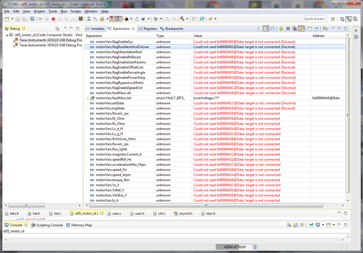
    C28xx_CPU1: Trouble Writing Memory Block at 0x402 on Page 1 of Length 0x1: (Error -1041 @ 0xFFFFFEFB) The debug probe reported an error. Confirm debug probe configuration and connections, reset the debug probe, and retry the operation. (Emulation package 8.4.0.00006) 28xx_CPU1: Trouble Halting Target CPU: (Error -1044 @ 0x0) The debug probe reported an error. Confirm debug probe configuration and connections, reset the debug probe, and retry the operation. (Emulation package 8.4.0.00006) C28xx_CPU1: Error: (Error -1044 @ 0x0) The debug probe reported an error. Confirm debug probe configuration and connections, reset the debug probe, and retry the operation. (Emulation package 8.4.0.00006)
    C28xx_CPU1: Unable to determine target status after 20 attempts C28xx_CPU1: Failed to remove the debug state from the target before  disconnecting. There may still be breakpoint op-codes embedded in program memory. It is recommended that you reset the emulator before you connect and reload your program before you continue debugging.


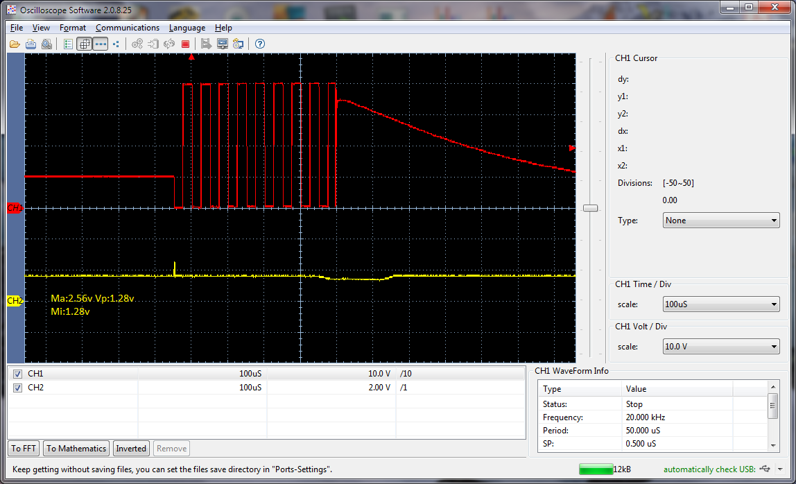
  • A voltage perspective (CH2) into GxADCAB, GxADCC shows there is no XDS110 anomaly. Also reduced SOH window on these 3 inputs from 14 clocks to 5 made no difference to stop XDS110 sudden disconnect. The USB cable has ferrite filter surrounding each end of the 3' cable length. Same cable was used with BoosXL drive kit for few weeks for unknown reason/s caught on fire during CCS real time debug via USB isolation, JP1,2,3 removed.

    Don't understand the schematic isolation region IC U3 as it was drawn, makes no sense (C1 net C2) as (C106 no nets C105). Seems left side (U3) +3v3  should go to VDD2 through barrier region for VDD1 (USB_VCC +3v3). If the PCB was designed as schematic shows it could explain the sudden XDS110 disconnects. Seemingly there should not be any NET between C1 or C2 and +3v3 should be placed on VDD2 to gain isolation through the barrier region.

    1. Was the schematic drawn correctly and or the launch pad PCB barrier region NETS properly configured?

    For example the same DC inverter connected EK-TM4C1294XL via USB (No isolation) XDS100 linked to run time GUI without these issues.  

    It seems the USB isolation region is not working as it should and BoostXL-drv8320rs external PGA filters white washes USB isolation issues. The x49c MCU is not POR, BOR or NMI fault states that can be visually noticed.


  • Also thought xds110 bounce could be dead band related shoot through but RED/FED are set for 180ns delay (hal.h) based on 10ns (100Mhz) PWM clock rate.

    The xds110 TM4c129x VDD has somewhat limited bulk caps 3 x 0.01uf, 2 x 0.1uf, 1 x 1uf . Our custom PCB TM4c1294 had to add 3.3uf on 3 VDD bus points to stop random POR. VDDC is about the same as our TM4C1294 1 x3.3uf, 2 x 0.1uf.

    Oddly custom PCB would not go as far into the PWM cycle as above scope capture, 9 x 50µs cycles prior to crashing XDS110.

  • Hi Kevin,

    Oddly when JP1, JP2, JP3 are removed XDS110 is not being isolated from the target sourced +3v3.

    This can be noticed as VBUS powers LED0 yet virtual COM4, COM5 are not present until the target side of isolation is provided +3v3. That is backwards isolation since U101 should be powering XDC110 TM4C129 MCU but does not.

    Stumbled onto this issue after enabling SCIA and attempting to print debug messages. Virtual COM4 is not present until the target has been powered. Seemingly jumpers should allow powering XDS110 from VBUS and not pass +3v3 across the isolation barrier for TMS320F280049c MCU.

    The x49c gets +3v3 from the Booster headers and should not pass 3v3 back to XDC110 when JP1,2,3 are removed. How it this possible that XDC110 is being powered +3v3 from the target side of isolation barrier when JP1, 2, 3 are removed?

  • Hi GI,

    For the LAUNCHXL-F280049C the XDS110 is on the DuT side. The USB interface from the computer to the XDS110 (U2) is isolated with U3 when JP1-3 are removed. The DuT / XDS110 side of the board is then meant to be powered by a separate isolated power source.

    Best,

    Kevin

  • Kevin Allen18 said:
    The DuT / XDS110 side of the board is then meant to be powered by a separate isolated power source.

    Yet if that was working as intended when +3v3 power is removed from target why do the XDS110 virtual COM ports vanish from device manager? If XDS110 is being powered via USB the virtual COM ports would remain in windows device manager, they do not!  3v3 Isolation is not being gained from the XDS110 perspective JP2 being removed. The XDS110 is sourcing 3v3 around JP2 from the target side of isolation.

  • I've tried everything to stop the XDS110 from bouncing CCS real time debug connection. Seemingly the +3v3 across JP2 has to be better isolated or has been compromised by odd PCB artwork. There is definitely something wrong with in the isolation boundary if XDS110 can source +3v3 from only the target (DUT) with JP2 has been removed. The point of rmoving JP2 is for the XDS110 to source 3v3 from the USB as any other connected device.

    "For the LAUNCHXL-F280049C the XDS110 is on the DuT side."

    That would be very odd (XDS/USB) isolation and the results can be seen as CCS drops the connection upon any little noise on to +3v3 target power. What is the point of removing JP2 and using the booster 3v3 power if the XDS110 is not being isolated as a USB device? Why not simply use the on board 3v3 (U101) to power all systems then. Something obviously was missed in this x49c PCB design and or not tested with jumper connected devices to J1-J8 headers.

  • GI,

    I think there's some confusion.

    Gl said:
    Yet if that was working as intended when +3v3 power is removed from target why do the XDS110 virtual COM ports vanish from device manager? If XDS110 is being powered via USB the virtual COM ports would remain in windows device manager, they do not!

    The XDS110 is not isolated with respect to the F28004x DuT. They share the same GND plane and PWR rail. So if 3.3V is removed from the F28004x it will be removed for the XDS110 (TM4C) as well.

    The isolation I'm mentioning is the USB connected to your PC is isolated from the XDS110 AND F28004x when JP1, 2, and 3 are removed.

    Gl said:
    Seemingly the +3v3 across JP2 has to be better isolated or has been compromised by odd PCB artwork.

    I'm not sure what you're meaning by the above.

    Best,

    Kevin