This thread has been locked.

If you have a related question, please click the "Ask a related question" button in the top right corner. The newly created question will be automatically linked to this question.

TMS320F28377S: ADC Testing and Validation

Part Number: TMS320F28377S
Other Parts Discussed in Thread: OPA320

What is the circuit that is used to validate that each of the ADC channels are working properly before shipping a product? I would like to design my input circuit as close as possible to this to reduce the chances that I am using ADC channels out of their operating spec.

  • Hi Trevor,

    The ADC is designed to be able to interface to a variety of inputs with different signal conditioning circuitry simultaneously. 

    Your main care-about here is ensuring that the ADC S+H duration (set by the ACQPS setting of the SOC logic) is long enough to allow input settling for whatever circuit you have driving the ADC.  Usually, you also have control of the design of the driving circuit, so you have lots of freedom to make this work correctly.

    To start, check out the "Choosing an Acquisition Window Duration" section of the TRM.  This gives simple (but conservative) guidance for the S+H based on the passives on the ADC input (R and C).  You'll also need the ADC input models in the device datasheet.  This analysis does not factor in the bandwidth of the driver (usually an op-amp) which could become the limiting factor.  

    To go more in depth, watch the videos at TI precision labs here about ADC driver design:  https://training.ti.com/ti-precision-labs-adcs-introduction-sar-adc-front-end-component-selection

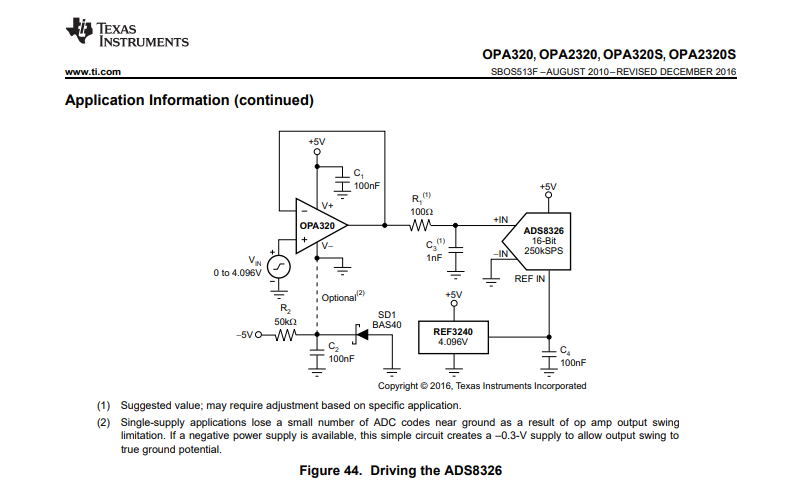
    And if you just need some starting point, try OPA320 in a voltage-follower configuration with Rs = 50 ohms and Cs = 300pF (R1 and C3 in the below diagram).  Even better if you add some low-pass filtering stage immediately before this driver stage.