This thread has been locked.

If you have a related question, please click the "Ask a related question" button in the top right corner. The newly created question will be automatically linked to this question.

SPI - MSP430F2274 with ADXL345

Other Parts Discussed in Thread: MSP430F2274, CC2500, MSP430F2132, MSP430F5438A, MSP430G2553

Hello everyone,

I am a newbie to MSP430 and SPI protocol. I read a lot about SPI online and also in the User Guide of MCU. The problem I am facing is described below;

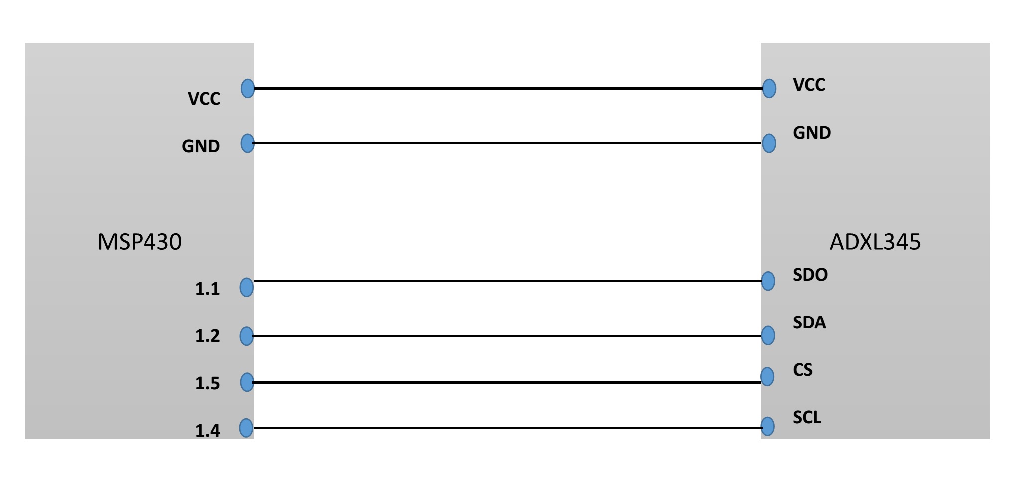
I am interfacing ADXL345 Accelerometer with MSP430F2274 via  3 wire SPI. I think I am doing all the initializing correctly, but I am not getting any useful data back.

I am trying to read the device ID of ADXL345 but I keep on getting 0xF2 instead of 0xE5. 

This is the data sheet for ADXL345; http://www.analog.com/static/imported-files/data_sheets/ADXL345.pdf

ADXL345 takes 16 bits of data at one time but the MCU can only clock out 8 bits in one transmission, I think this creates a timing difference in the communication and hence

I don’t get what I want. Below is the code I am trying to use:

#include "msp430x22x4.h"

volatile unsigned char Data;
volatile int i;
void main(void)
{
  WDTCTL = WDTPW + WDTHOLD;                                           // Stop watchdog timer
  P3SEL |= 0x31;                                                                             // P3.0,P3.4,P3.5 USCI_A0 option select
  P3DIR |= 0x40;                                                                             // P3.6 output direction
  P4DIR |= BIT3;                                                                             // Used to provide power to the Accelerometer 
  P4OUT &= ~BIT3;     
   

                                      // SPI initialization 
  UCA0CTL0 |= UCCKPH + UCCKPL + UCMSB + UCMST + UCSYNC;              // 3-pin, 8-bit SPI master
  UCA0CTL1 |= UCSSEL_2;                                                       // Select SMCLK as CLK
  UCA0BR0 |= 0x02;
  UCA0BR1 = 0;                             
  UCA0MCTL = 0;
  UCA0CTL1 &= ~UCSWRST;                                                   // **Initialize USCI state machine**
  P4OUT |= BIT3;                                                                          // Turn the Accelerometer on
  while(1)
  {
 
    P3OUT  &= ~0x40;                                                                           // Chip select active low
    for(i = 0xFFFF; i > 0; i--);                                                             // Delay
    IFG2 &= ~UCA0RXIFG;                                                              // Clear int flag
    while ((IFG2 & UCA0TXIFG) == 0);
    UCA0TXBUF = 0xC0;                                                               // Read Dev ID
    IFG2 &= ~UCA0RXIFG;
    //while ((IFG2 & UCA0TXIFG) == 0);                                     // TXBUF ready?                    
    UCA0TXBUF = 0x45;
    while ((IFG2 & UCA0TXIFG) == 0);                                      // TXBUF ready?  
    P3OUT |= 0x40;                                                                      // End Transmission
    while ((IFG2 & UCA0RXIFG) == 0);                                       // RXBUF ready?
    Data = UCA0RXBUF;                                                               // Move value
  
  }
}

Somebody please help me on this.

Thanks.

  • istemihan90 said:
    You can configure for your pins of the chip you re using. When you read the datasheet of ADXL carefully, you will see you need to set MSB as 1 for reading and 0 for Writting.


    Does that mean that we should not set the Bit 5 in the UCA0CTL0  register in order to write to reg. value from the ADXL345?

    Thanks 

  • Murtadha A said:
    Does that mean that we should not set the Bit 5 in the UCA0CTL0  register in order to write to reg. value from the ADXL345?

    The UCMSB bit (UCA0CTL0.5) defines the order in which the bits in UCA0TXBUF are sent. The bit stream can start with the LSB or the MSB. MSB first is the usual way.

    However, what istemihan90 referred to was that the MSB must be set to 0 for writing and 1 for reading. That means, the value you write to UCA0TXBUF for the register number must have its MSB clear (0b0xxxxxxx) if you want to write to that register and set (0b1xxxxxxx) if you want to read from it.

  • Thank you Jens-Michael
    I have two questions:
    1)Why they reorganize the bits such that they send 0x08 instead of 0x00 (0x00 is the register in which the acceleromter ID is stored)?

    2) why do they send a dummy byte when using the SPI (the 0xFF)?
  • Murtadha A said:
    Why they reorganize the bits such that they send 0x08 instead of 0x00

    I guess you mean 0x80?

    The address byte you send to the ADXL is organized as 0xCBAAAAAA where A is the register address, B is the multi-byte flag (for subsequent reads or writes without sending  anew register address each time) and C is the read/write bit. C must be set when you want to read a register (even if the register is read-only anyway) an clear when you write to that register (which would do nothing if the register is read-only).

    So sending 0x80 as address byte means that you want to read from register 0 while sending 0x00 would mean that you want to write to register 0.

    The dummy byte is required for the transfer. SPI is a synchronous master-clocked master/slave protocol. That means, to have a bit sent in any direction, the master needs to create a clock pulse. Also, the master may not create additional clock pulses beyond the number of bits to be tranferred. So the master must know when to generate how many clock pulses. In the MSP USCI, this is done by writing to TXBUF. Writing to TXBUF makes the USCI generate 8 clock pulses during which the byte written to TXBUF is sent and a byte is received from the selected slave. SPI always sends and receives at the same time (at different clock edges, this is why you can configure clock and polarity to match the slave). If you don't want to send anything, you send 0xff. During the 8 clock cycles, the slave will send out 8 bits while receiving 8 bits. Depending on the protocol (in this case, transmitting address ybte, sending data byte or receiving data byte), the slave will ignore these received bits or will send 8 dummy bits while receiving 8 significant bits.Or both (but that's rather uncommon except for cascaded shift register slaves). If you hadn't connected the master out/slave in (MOSI) line, the slave would still 'receive' 0xff.


    So to receive a byte, you have to send a dummy byte. And when sending a byte, you'll receiving a dummy byte. When you are done sending the address byte, RXIFG will be set as you received a dummy byte from the slave at the same time which you have to discard (at least clear RXIFG manually). The response from the slave with the read register content will arrive after the dummy byte has been sent (when RXIFG is set a second time). This enterleaved action often confuses people, but looking an SPI timing diagram, it is clear what happens (and how).

    It should be noted that the bits are sent and received at different clock edges, so depending on the speed of the SPI bus in relation to MCLK, RX and TX interrupts may come in different order. Also, there is double-buffering for RXBUF and TXBUF. When RXIFG is set, it means that a byte has arrived, but another byte may be already coming in. And when TXIFG is set, it measn that TXBUF is empty, but the last byte written to TXBU may still be in the process of being clocked out. To be sure that the last byte has been sent (and received), UCBUSY must be checked. Only then, the chip select signal to the slave may be safely un-asserted.

    On I2C, which is also a synchronous master-clocked master/slave protocol, there is only one direction active at a time. And you tell the USCI beforehand whether to send or receive and when a transfer is complete. So there is no need for sending dummy bytes. But it has other pitfalls and is significantly slower than SPI.

  • Mr. Gross

    I am always thankful for your replies!

    I tested this piece of code for reading the ADXL ID and it works fine.

    Kindly see the code below. You can see that I am using while(1) to keep reading the 1st byte of x acceleration (register 0x32, to be read as 0xB2). But I am getting the same value 0xF9? even if I move the acceleromter and re load the code , I am still getting 0xF9. Would you please take a look and advice if I am doing something wrong.

    And for reading 6 bytes, now I know that I should set the B bit, but how can I specify that I want to read 6 bytes starting from 0xB2? should I use a function that takes care of sending a string of bytes?  

    //SPI communication: 0xCBAAAAAA
    
    //B is the multi-byte flag (for subsequent reads or writes without sending  anew register address each time)
    
    //C is the read/write bit
    //C must be set when you want to read a register (even if the register is read-only anyway)
    //and clear when you write to that register (which would do nothing if the register is read-only).
    #include <msp430g2553.h>
    
    volatile char received_byte1 = 0;
    volatile char received_byte2 = 0;
    volatile char received_byte3 = 0;
    volatile char received_byte4 = 0;
    volatile char received_byte5 = 0;
    volatile char ACC_X0 = 0;
    unsigned int i, a=0, b=0, c=0, d=0;
    
    void spi_conf(void);
    void general_clock_cong(void);
    void spi_read(void);
    void spi_read_acc(void);
    void spi_write(void);
    
    
    void main(void){
    
    	while (1){
    
    	WDTCTL = WDTPW + WDTHOLD; // Stop watchdog timer
            general_clock_cong();
    
            spi_conf();
            spi_write();
    
            //spi_read();
            spi_read_acc();
            }
    }
    
    void general_clock_cong(void){
    
    DCOCTL = CAL_DCO_16MHZ;
    BCSCTL1 = CAL_BC1_16MHZ;
    }
    
    void spi_conf(void){
    
    UCA0CTL1 = UCSWRST; // Reset
    UCA0CTL0 = UCCKPL + UCMSB + UCMST + UCSYNC; // 3-pin, 8-bit SPI master
    UCA0CTL1 |= UCSSEL_2 ; // USCI clock source select. (SMCLK)
    UCA0BR0 = 128; // Baud Rate
    UCA0BR1 = 0; // Baud Rate
    UCA0CTL1 &= ~UCSWRST; // clear reset
    
    P1SEL = (BIT1 + BIT2 + BIT4); // Set SPI CLK, MOSI and MISO
    P1SEL2 = (BIT1 + BIT2 + BIT4);
    P1DIR = BIT5; // BIT 5 SPI EN, BIT0 LED
    }
    
    void spi_read(void){
    
    //P1OUT |= BIT5;
    P1OUT &= ~BIT5;               // BIT 5 is CS
    
    while (!(IFG2&UCA0TXIFG)); // Wait for TXBUF ready
    UCA0TXBUF = 0x80; // Read the ID register
    a=a+1;
    while(!(IFG2 & UCA0RXIFG)); // Wait for RXBUF ready
    received_byte1 = UCA0RXBUF;
    if (received_byte1==0xE5)
    	b=b+1;
    
    while (!(IFG2&UCA0TXIFG)); // Wait for TXBUF ready
    UCA0TXBUF = 0xFF; // Send dummy byte
    while(!(IFG2 & UCA0RXIFG)); // Wait for RXBUF ready
    received_byte2 = UCA0RXBUF;
    
    while (!(UCB0STAT & UCBUSY)==0);
    P1OUT |= BIT5;
    }
    
    void spi_read_acc(void){ //to read the acceleration data
    
    //P1OUT |= BIT5;
    P1OUT &= ~BIT5;               // BIT 5 is CS
    
    while (!(IFG2&UCA0TXIFG)); // Wait for TXBUF ready
    UCA0TXBUF = 0xB2; // Read the acc X0 register (0x32)
    
    while(!(IFG2 & UCA0RXIFG)); // Wait for RXBUF ready
    ACC_X0 = UCA0RXBUF;
    
    while (!(IFG2&UCA0TXIFG)); // Wait for TXBUF ready
    UCA0TXBUF = 0xFF; // Send dummy byte
    while(!(IFG2 & UCA0RXIFG)); // Wait for RXBUF ready
    
    while (!(UCB0STAT & UCBUSY)==0);
    P1OUT |= BIT5;
    }
    
    void spi_write(void){
    
    //P1OUT |= BIT5;
    P1OUT &= ~BIT5;               // BIT 5 is CS
    
    while (!(IFG2&UCA0TXIFG)); // Wait for TXBUF ready
    UCA0TXBUF = 0x2D; // We want to write to the power register
    while(!(IFG2 & UCA0RXIFG)); // Wait for RXBUF ready
    
    while (!(IFG2&UCA0TXIFG)); // Wait for TXBUF ready
    UCA0TXBUF = 0x10; // Write the 0x10 to the power register
    while(!(IFG2 & UCA0RXIFG)); // Wait for RXBUF ready
    
    while (!(IFG2&UCA0TXIFG)); // Wait for TXBUF ready
    UCA0TXBUF = 0xFF; // Send dummy byte
    while(!(IFG2 & UCA0RXIFG)); // Wait for RXBUF ready
    received_byte2 = UCA0RXBUF;
    
    while (!(IFG2&UCA0TXIFG)); // Wait for TXBUF ready
    UCA0TXBUF = 0x2D; // We want to write to the power register
    while(!(IFG2 & UCA0RXIFG)); // Wait for RXBUF ready
    
    while (!(IFG2&UCA0TXIFG)); // Wait for TXBUF ready
    UCA0TXBUF = 0x08; // Write the 0x08 to the power register to put it in measure mode
    while(!(IFG2 & UCA0RXIFG)); // Wait for RXBUF ready
    
    while (!(IFG2&UCA0TXIFG)); // Wait for TXBUF ready
    UCA0TXBUF = 0xFF; // Send dummy byte
    while(!(IFG2 & UCA0RXIFG)); // Wait for RXBUF ready
    received_byte2 = UCA0RXBUF;
    
    while (!(UCB0STAT&UCBUSY)==0);
    P1OUT |= BIT5;
    }


  • >while (!(IFG2&UCA0TXIFG)); // Wait for TXBUF ready
    >UCA0TXBUF = 0xB2; // Read the acc X0 register (0x32)
    >while(!(IFG2 & UCA0RXIFG)); // Wait for RXBUF ready
    >ACC_X0 = UCA0RXBUF;
    >while (!(IFG2&UCA0TXIFG)); // Wait for TXBUF ready
    >UCA0TXBUF = 0xFF; // Send dummy byte
    >while(!(IFG2 & UCA0RXIFG)); // Wait for RXBUF ready

    The ACC_X0 data comes back in the following byte (see Figure 38). That is, it's available only at the end of this sequence, after sending the dummy byte.

    More generally: To follow this pattern, you should make a point of always reading UCA0RXBUF after waiting for UCA0RXIFG, or you'll be off-by-one later. If you're not interested in the contents, you can do something like "(void)UCA0RXBUF;" to make it clear you're reading it and throwing it away. I usually wrap this sequence (wait-write-wait-read) into a separate function so I don't forget.
  • Bruce already said it, but maybe not detailed enough to really understand the mistake here.

    Let's write down what happens when, starting with a freshly initialized USCI module.

    > while (!(IFG2&UCA0TXIFG)); // Wait for TXBUF ready

    At this point, UCA0TXIFG is set, as it is instantly set as soon as the USCI is initialized and UCSWRST is cleared.

    > UCA0TXBUF = 0xB2; // Read the acc X0 register (0x32)

    This clears UCA0TXIFG. with the next clock pulse, 0x2D is moved to the output shift register and UCA0TXIFG is set again, indicating that UCA0TXBUF can take a second byte now (which will sit there until the previous one is done sending). This double-buffering enables higher throughput on high SPI clock rates.

    > while(!(IFG2 & UCA0RXIFG)); // Wait for RXBUF ready

    While  the 0xb2 is being sent, the USCI will at the same time receive 8 bits. If the slave doesn't send anything, the USCI will receive 0xff. Or whatever signal level the MISO line will have. The slave can't send the register content right now, as it hasn't received the read request (it is still sending). Once UCA0RXIFG is set, the USCI received a DUMMY byte.

    > ACC_X0 = UCA0RXBUF;

    You read the dummy byte, not the ACC-X0 value here. You have to read UCA0RXBUF or at least manually clear UCA0RXIFG here, so you can see when the next byte is received, the one you want.
    You can make a dummy read by simply writing

    UCA0RXBUF;

    Since this is a volatile memory location, teh compiler will generate a read access (which is what you want) even if you do not do anything with the read value.

    > while (!(IFG2&UCA0TXIFG)); // Wait for TXBUF ready

    Well, since the USCI was idle at start, TXIFG is already set here. But waiting won't hurt

    > UCA0TXBUF = 0xFF; // Send dummy byte

    This starts sending a dummy byte and at the same time starts receiving the requested data byte.

    > while(!(IFG2 & UCA0RXIFG)); // Wait for RXBUF ready

    Here you wait for the data byte being received. That's okay. But after this line, you should read the data byte:

    ACC_X0=UCA0RXBUF; // this time, we get the ACC vlaue, not the dummy byte.

    Then you wait for UCBUSY clear before you de-assert CS. Since you already got what you want (the byte was received), the wait is not 100% necessary. However, it is a good habit, as it deals with all situations and software protocol variants. Sometimes, a transfer from (and more often: to) a slave has side-effects if CS is de-asserted too fast. Even if you already got what you want, the slave might consider the transfer incomplete and skip incrementing a counter or updating a register as intended. Or even discard the received byte instead of writing it. Sometimes, an additional delay even after completing the transfer is required (especially on write access to non-volatile registers or flash cells).
    However, after UCBUSY is clear, UCA0TXIFG is set, as a clear UCBUSy implies that both, UCA0TXBUF and the output shift register are both empty.

    The above sequence also applies to reading the ID register 0.

    For writing to a register, you always get dummy bytes for ever byte you send, but you probably won't care. However, ensure that you clear UCA0RXIFG after the transfer is competed (or before you start a new read operation).

    For reading all ACC registers in a block, send 0xf2 as register address, then send another dummy byte for each additional register and you'll get another data byte. If you always wait for the IFG bits being set, you won't have problems. But this is slower than necessary. You either have a (physical) transfer or handle the data/prepare the next byte. Instead of handling the data while the next transfer is already in progress.  When you want fastest throughput or when you move to interrupt-driven operation, you'll get/handle the interrupts when and in the order they happen and not when you check for them. Then you'll have to take care of the interleaved operation (one byte waiting in TXBUF while the previous one is being sent and/received, receiving a byte in RXBUF in response of the penultimate byte you wrote to TXBUF)

    SPI - MSP430F2274 with ADXL345

  • Jens-Michael and Bruce
    Many thanks for your replies!

    I modified the code as below. However, I am getting 0x00 now in for the ACC_X0. I followed your recommendations, so please take a look at the code and advice.
    Many thanks and happy thanksgiving 

    //SPI communication: 0xCBAAAAAA
    
    //B is the multi-byte flag (for subsequent reads or writes without sending  anew register address each time)
    
    //C is the read/write bit
    //C must be set when you want to read a register (even if the register is read-only anyway)
    //and clear when you write to that register (which would do nothing if the register is read-only).
    #include <msp430g2553.h>
    
    volatile char received_byte1 = 0;
    volatile char received_byte2 = 0;
    volatile char received_byte3 = 0;
    volatile char received_byte4 = 0;
    volatile char received_byte5 = 0;
    volatile char ACC_X0 = 0;
    unsigned int i, a=0, b=0, c=0, d=0;
    
    void spi_conf(void);
    void general_clock_cong(void);
    void spi_read(void);
    void spi_read_acc(void);
    void spi_write(void);
    
    
    void main(void){
    
    while (1){
    
    WDTCTL = WDTPW + WDTHOLD; // Stop watchdog timer
    general_clock_cong();
    
    spi_conf();
    
    spi_write(); //for setting the power mode of the aceelerometer
    
    spi_read_acc(); //to read the acceleration
    }
    }
    
    void general_clock_cong(void){
    
    DCOCTL = CAL_DCO_16MHZ;
    BCSCTL1 = CAL_BC1_16MHZ;
    }
    
    void spi_conf(void){
    
    UCA0CTL1 = UCSWRST; // Reset
    UCA0CTL0 = UCCKPL + UCMSB + UCMST + UCSYNC; // 3-pin, 8-bit SPI master
    UCA0CTL1 |= UCSSEL_2 ; // USCI clock source select. (SMCLK)
    UCA0BR0 = 128; // Baud Rate
    UCA0BR1 = 0; // Baud Rate
    UCA0CTL1 &= ~UCSWRST; // clear reset
    
    P1SEL = (BIT1 + BIT2 + BIT4); // Set SPI CLK, MOSI and MISO
    P1SEL2 = (BIT1 + BIT2 + BIT4);
    P1DIR = BIT5; // BIT 5 SPI EN, BIT0 LED
    }
    
    //////////////////////////////////////////////////////////////////////
    void spi_read(void){
    
    P1OUT &= ~BIT5;               // BIT 5 is CS
    
    while (!(IFG2&UCA0TXIFG)); // Wait for TXBUF ready
    UCA0TXBUF = 0x80; // Read the ID register
    a=a+1;
    while(!(IFG2 & UCA0RXIFG)); // Wait for RXBUF ready
    received_byte1 = UCA0RXBUF;
    if (received_byte1==0xE5)
    	b=b+1;
    
    while (!(IFG2&UCA0TXIFG)); // Wait for TXBUF ready
    UCA0TXBUF = 0xFF; // Send dummy byte
    while(!(IFG2 & UCA0RXIFG)); // Wait for RXBUF ready
    received_byte2 = UCA0RXBUF;
    
    while (!(UCB0STAT & UCBUSY)==0);
    P1OUT |= BIT5;
    }
    
    /////////////////////////////////////////////////////////////////////////
    void spi_read_acc(void){ //to read the acceleration data
    
    P1OUT &= ~BIT5;               // BIT 5 is CS
    
    while (!(IFG2&UCA0TXIFG)); // Wait for TXBUF ready
    UCA0TXBUF = 0xB2; // Read the acc X0 register (0x32)
    while(!(IFG2 & UCA0RXIFG)); // Wait for RXBUF ready
    UCA0RXBUF; //not interested in the content
    
    while (!(IFG2&UCA0TXIFG)); // Wait for TXBUF ready
    UCA0TXBUF = 0xFF; // Send dummy byte
    while(!(IFG2 & UCA0RXIFG)); // Wait for RXBUF ready
    ACC_X0 = UCA0RXBUF; //we want this
    
    while (!(UCB0STAT & UCBUSY)==0);
    P1OUT |= BIT5;
    }
    
    ///////////////////////////////////////////////////////////////////
    void spi_write(void){
    
    P1OUT &= ~BIT5;               // BIT 5 is CS
    
    while (!(IFG2&UCA0TXIFG)); // Wait for TXBUF ready
    UCA0TXBUF = 0x2D; // We want to write to the power register
    while(!(IFG2 & UCA0RXIFG)); // Wait for RXBUF ready
    IFG2 &= ~UCA0RXIFG;
    
    while (!(IFG2&UCA0TXIFG)); // Wait for TXBUF ready
    UCA0TXBUF = 0x10; // Write the 0x10 to the power register
    while(!(IFG2 & UCA0RXIFG)); // Wait for RXBUF ready
    IFG2 &= ~UCA0RXIFG;
    
    while (!(IFG2&UCA0TXIFG)); // Wait for TXBUF ready
    UCA0TXBUF = 0xFF; // Send dummy byte
    while(!(IFG2 & UCA0RXIFG)); // Wait for RXBUF ready
    IFG2 &= ~UCA0RXIFG;
    
    while (!(IFG2&UCA0TXIFG)); // Wait for TXBUF ready
    UCA0TXBUF = 0x2D; // We want to write to the power register
    while(!(IFG2 & UCA0RXIFG)); // Wait for RXBUF ready
    IFG2 &= ~UCA0RXIFG;
    
    while (!(IFG2&UCA0TXIFG)); // Wait for TXBUF ready
    UCA0TXBUF = 0x08; // Write the 0x08 to the power register to put it in measure mode
    while(!(IFG2 & UCA0RXIFG)); // Wait for RXBUF ready
    IFG2 &= ~UCA0RXIFG;
    
    while (!(IFG2&UCA0TXIFG)); // Wait for TXBUF ready
    UCA0TXBUF = 0xFF; // Send dummy byte
    while(!(IFG2 & UCA0RXIFG)); // Wait for RXBUF ready
    IFG2 &= ~UCA0RXIFG;
    
    while (!(UCB0STAT&UCBUSY)==0);
    P1OUT |= BIT5;
    }


  • When writing data, you mus tnot send a dummy byte. You send the real data byte instead and receive dummy bytes for them.
    In your code, after sending 0x10 to the power register, you start a repeaded read on Register 0x3f (by sending 0xff). You never put the ADXL into power mode as your 0x2d as well as the 0x08 are taken as dummy bytes for sequential reads.
    Remove the two dummy byte writes in spi_write(). Also, you don't need to wait for UCA0RXIFG. You know that you're only writing and never care for the incoming dummy bytes. (well, some slaves may send a generic status byte instead of a real dummy byte, but in your case, you can simply ignore the received part). Only at the end of the write, make sure that you clear UXA0RXIFG before you exit the function (when UCBUSY is clear).

    btw: when reading the ID register, you still read the wrong byte. YOur received_byte1 is the dummy byte received while sending the ID register read request. received_byte2 is the ID.
  • Sorry guys, I am bothering you with my e-mails. But I did not got it to work. Now I am getting 0x3C  for ACC_X0, even when I pause the program and run it again. i.e. the value does not change, even if I change the orientation.

    The code is as shown below. I also attach the connection diagram to take a look at for a double check .

    Many thanks

    //SPI communication: 0xCBAAAAAA
    
    //B is the multi-byte flag (for subsequent reads or writes without sending  anew register address each time)
    
    //C is the read/write bit
    //C must be set when you want to read a register (even if the register is read-only anyway)
    //and clear when you write to that register (which would do nothing if the register is read-only).
    #include <msp430g2553.h>
    
    volatile char received_byte1 = 0;
    volatile char received_byte2 = 0;
    volatile char received_byte3 = 0;
    volatile char received_byte4 = 0;
    volatile char received_byte5 = 0;
    char ACC_X0 = 0;
    char ADXL_ID = 0;
    
    unsigned int i, a=0, b=0, c=0, d=0;
    
    void spi_conf(void);
    void general_clock_cong(void);
    void spi_read(void);
    void spi_read_acc(void);
    void spi_write(void);
    
    
    void main(void){
    
    while (1){
    
    WDTCTL = WDTPW + WDTHOLD; // Stop watchdog timer
    general_clock_cong();
    
    spi_conf();
    
    spi_write(); //for setting the power mode of the aceelerometer
    
    spi_read_acc(); //to read the acceleration
    }
    }
    
    void general_clock_cong(void){
    
    DCOCTL = CAL_DCO_16MHZ;
    BCSCTL1 = CAL_BC1_16MHZ;
    }
    
    void spi_conf(void){
    
    UCA0CTL1 = UCSWRST; // Reset
    UCA0CTL0 = UCCKPL + UCMSB + UCMST + UCSYNC; // 3-pin, 8-bit SPI master
    UCA0CTL1 |= UCSSEL_2 ; // USCI clock source select. (SMCLK)
    UCA0BR0 = 128; // Baud Rate
    UCA0BR1 = 0; // Baud Rate
    UCA0CTL1 &= ~UCSWRST; // clear reset
    
    P1SEL = (BIT1 + BIT2 + BIT4); // 1.1: SDO, 1.2: SDA, 1.4: SCL
    P1SEL2 = (BIT1 + BIT2 + BIT4);
    P1DIR = BIT5; // 1.5: CS
    }
    
    //////////////////////////////////////////////////////////////////////
    void spi_read(void){
    
    P1OUT &= ~BIT5;               // BIT 5 is CS
    
    while (!(IFG2&UCA0TXIFG)); // Wait for TXBUF ready
    UCA0TXBUF = 0x80; // Read the ID register
    a=a+1;
    while(!(IFG2 & UCA0RXIFG)); // Wait for RXBUF ready
    received_byte1 = UCA0RXBUF;
    UCA0RXBUF; //not interested in the content
    //	b=b+1;
    
    while (!(IFG2&UCA0TXIFG)); // Wait for TXBUF ready
    UCA0TXBUF = 0xFF; // Send dummy byte
    while(!(IFG2 & UCA0RXIFG)); // Wait for RXBUF ready
    ADXL_ID = UCA0RXBUF;
    
    while (!(UCB0STAT & UCBUSY)==0);
    P1OUT |= BIT5;
    }
    
    /////////////////////////////////////////////////////////////////////////
    void spi_read_acc(void){ //to read the acceleration data
    
    P1OUT &= ~BIT5;               // BIT 5 is CS
    
    while (!(IFG2&UCA0TXIFG)); // Wait for TXBUF ready
    UCA0TXBUF = 0xB2; // Read the acc X0 register (0x32)
    while(!(IFG2 & UCA0RXIFG)); // Wait for RXBUF ready
    UCA0RXBUF; //not interested in the content
    IFG2 &= ~UCA0RXIFG;
    
    while (!(IFG2&UCA0TXIFG)); // Wait for TXBUF ready
    UCA0TXBUF = 0xFF; // Send dummy byte
    while(!(IFG2 & UCA0RXIFG)); // Wait for RXBUF ready
    ACC_X0 = UCA0RXBUF; //we want this
    
    IFG2 &= ~UCA0RXIFG;
    while (!(UCB0STAT & UCBUSY)==0);
    P1OUT |= BIT5;
    }
    
    ///////////////////////////////////////////////////////////////////
    void spi_write(void){
    
    P1OUT &= ~BIT5;               // BIT 5 is CS
    
    while (!(IFG2&UCA0TXIFG)); // Wait for TXBUF ready
    UCA0TXBUF = 0x2D; // We want to write to the power register
    
    while (!(IFG2&UCA0TXIFG)); // Wait for TXBUF ready
    UCA0TXBUF = 0x00; // Write the 0x00 to the power register
    ///--------------------------------------------------------
    while (!(IFG2&UCA0TXIFG)); // Wait for TXBUF ready
    UCA0TXBUF = 0x2D; // We want to write to the power register
    
    while (!(IFG2&UCA0TXIFG)); // Wait for TXBUF ready
    UCA0TXBUF = 0x10; // Write the 0x10 to the power register
    ///--------------------------------------------------------
    while (!(IFG2&UCA0TXIFG)); // Wait for TXBUF ready
    UCA0TXBUF = 0x2D; // We want to write to the power register
    
    while (!(IFG2&UCA0TXIFG)); // Wait for TXBUF ready
    UCA0TXBUF = 0x08; // Write the 0x08 to the power register to put it in measure mode
    ///---------------------------------------------------------
    while (!(UCB0STAT&UCBUSY)==0);
    IFG2 &= ~UCA0RXIFG;
    
    P1OUT |= BIT5;
    }

  • In your graphic, I noticed the label 'SDA' on the ADXL side. It should actually read SDI (serial data in) and matches the MSP's SIMO pin while SDO matches SOMI. YOur wiring is correct.
    It should be nothed that '3-wire-SPI' refers to different things on the ADXL and MSP. On ADXL it means you have clock, one data line and a chip select (the MSP doesn't support this), while the MSP doesn't count the chip select (every slave has its own , so only the shared lines on the bus are counted). MSP's 3-wire mode matches what ADXL calls 4-wire mode.

    The code looks good too, regarding the general SPI operation. One thing I noticed: when initializing P1DIR.5, the content of P1OUT is undefined. So the pin may switch to high or low. Furthermore, before this, the pin is high-impedance, which is an undefined state on the ADXL. It may be that the ADXL is selected from this moment on.
    To be on the safe side, you should set P1OUT.5 to 0, P1DIR.5 to 1 and then P1OUT.5 to 1. This gives the CS line a defined state and terminates any assumed (bogus) transfer.

    The clock speed is quite low (128kHz on 16MHz SMCLK). The ADXL can cope with 5MHz. But that's no problem, as long as you only use the 200Hz output data rate and below (default is 100Hz, so this is okay). For the higher output rates, you'll need a higher SPI clock.

    Why do you send 0x10 ot the power register? This enables auto-sleep, which you likely doN't want at this time and which may have side-effects depending on other config settings (I didn't check the defaults). You may/should skip this step.

    Default is +-2g range, so teh values read must be clipped (whatever this means, I did read this in the register 0x31 description)

    But the main problem is:
    It takes some time after enabling measure mode to get the first valid result. On 100Hz output rate, I would assume 10ms before the first result is ready. 10ms on 128kHz SPi clock means it takes the time to transfer 160 bytes on SPI before the first sample is ready.
    But you instantly read the data. And on each program loop, you exit and re-enter measure mdoe, so the 10ms delay starts again on each loop. This way, there will never be a measure cycle completed and the registers will never get any value apart from the power-von content.

    You may add a delay funciton that continually reads register 0x30 (using address 0x70 followed by a loop of dummy writes) until the returned byte (except for the first, which is the dummy response) has the MSB set (DATA_READY). This busy-waiting loop would delay the progress of the code until data has been measured. The DATA_READY-bit is cleared when you read the register, whether you actually read the data or not. So when it is set next time, the next set of data is available.
  • Thank you Mr. Gross, I appreciate your help

    The program is working after following your suggestions.

    I made few changes as well, now I am reading the acceleration of X, Y, Z and I made the SPI faster as I that was not clear for me before. Also, as you will see below, I put the accelrometer into sleep after reading the acceleration and disable the SPI (by enabling UCSWRST). 
    Thank you again 

    //SPI communication: 0xCBAAAAAA
    
    //B is the multi-byte flag (for subsequent reads or writes without sending  anew register address each time)
    
    //C is the read/write bit
    //C must be set when you want to read a register (even if the register is read-only anyway)
    //and clear when you write to that register (which would do nothing if the register is read-only).
    #include <msp430g2553.h>
    
    char ACC_X0 = 0, ACC_Y0 = 0, ACC_Z0 = 0;
    char ACC_X1 = 0, ACC_Y1 = 0, ACC_Z1 = 0;
    char ADXL_ID = 0;
    
    unsigned int i, a=0, b=0, c=0, d=0;
    
    void spi_conf(void);
    void general_clock_cong(void);
    void spi_read(void);
    void spi_read_acc(void);
    void spi_write(void);
    void delay_ms(unsigned int);
    void ADXL345_sleep(void);
    
    void main(void){
    
    while (1){
    
    WDTCTL = WDTPW + WDTHOLD; // Stop watchdog timer
    general_clock_cong();
    
    spi_conf();
    
    spi_write(); //for setting the power mode of the aceelerometer
    
    spi_read_acc(); //to read the acceleration
    ADXL345_sleep();
    UCA0CTL1 = UCSWRST; // Enable --USCI in reset state
    
    }
    }
    
    void general_clock_cong(void){
    
    DCOCTL = CALDCO_8MHZ; //CAL_DCO_16MHZ;
    BCSCTL1 = CALBC1_8MHZ; //CAL_BC1_16MHZ;
    }
    
    void spi_conf(void){
    
    UCA0CTL1 = UCSWRST; // Reset
    UCA0CTL0 = UCCKPL + UCMSB + UCMST + UCSYNC; // 3-pin, 8-bit SPI master
    UCA0CTL1 |= UCSSEL_2 ; // USCI clock source select. (SMCLK)
    UCA0BR0 = 0x02; // Baud Rate SMCLK/2 (4MHz)
    UCA0BR1 = 0; // Baud Rate
    UCA0CTL1 &= ~UCSWRST; // clear --reset for operation
    
    P1SEL = (BIT1 + BIT2 + BIT4); // 1.1: SDO, 1.2: SDA, 1.4: SCL
    P1SEL2 = (BIT1 + BIT2 + BIT4);
    
    P1OUT &= ~BIT5;
    P1DIR = BIT5; // 1.5: CS
    P1OUT |= BIT5;
    
    }
    
    //////////////////////////////////////////////////////////////////////
    void spi_read(void){
    
    P1OUT &= ~BIT5;               // BIT 5 is CS
    
    while (!(IFG2&UCA0TXIFG)); // Wait for TXBUF ready
    UCA0TXBUF = 0x80; // Read the ID register
    a=a+1;
    while(!(IFG2 & UCA0RXIFG)); // Wait for RXBUF ready
    UCA0RXBUF; //not interested in the content
    
    while (!(IFG2&UCA0TXIFG)); // Wait for TXBUF ready
    UCA0TXBUF = 0xFF; // Send dummy byte
    while(!(IFG2 & UCA0RXIFG)); // Wait for RXBUF ready
    ADXL_ID = UCA0RXBUF;
    
    while (!(UCB0STAT & UCBUSY)==0);
    P1OUT |= BIT5;
    }
    
    /////////////////////////////////////////////////////////////////////////
    void spi_read_acc(void){ //to read the acceleration data
    
    P1OUT &= ~BIT5;               // BIT 5 is CS
    
    while (!(IFG2&UCA0TXIFG)); // Wait for TXBUF ready
    UCA0TXBUF = 0xF2; // Read the acc X0 register (0x32)
    while(!(IFG2 & UCA0RXIFG)); // Wait for RXBUF ready
    UCA0RXBUF; //not interested in the content
    //IFG2 &= ~UCA0RXIFG;
    
    while (!(IFG2&UCA0TXIFG)); // Wait for TXBUF ready
    UCA0TXBUF = 0xFF; // Send dummy byte
    while(!(IFG2 & UCA0RXIFG)); // Wait for RXBUF ready
    ACC_X0 = UCA0RXBUF; //we want this
    
    while (!(IFG2&UCA0TXIFG)); // Wait for TXBUF ready
    UCA0TXBUF = 0xFF; // Send dummy byte
    while(!(IFG2 & UCA0RXIFG)); // Wait for RXBUF ready
    ACC_X1 = UCA0RXBUF; //we want this
    
    while (!(IFG2&UCA0TXIFG)); // Wait for TXBUF ready
    UCA0TXBUF = 0xFF; // Send dummy byte
    while(!(IFG2 & UCA0RXIFG)); // Wait for RXBUF ready
    ACC_Y0 = UCA0RXBUF; //we want this
    
    while (!(IFG2&UCA0TXIFG)); // Wait for TXBUF ready
    UCA0TXBUF = 0xFF; // Send dummy byte
    while(!(IFG2 & UCA0RXIFG)); // Wait for RXBUF ready
    ACC_Y1 = UCA0RXBUF; //we want this
    
    while (!(IFG2&UCA0TXIFG)); // Wait for TXBUF ready
    UCA0TXBUF = 0xFF; // Send dummy byte
    while(!(IFG2 & UCA0RXIFG)); // Wait for RXBUF ready
    ACC_Z0 = UCA0RXBUF; //we want this
    
    while (!(IFG2&UCA0TXIFG)); // Wait for TXBUF ready
    UCA0TXBUF = 0xFF; // Send dummy byte
    while(!(IFG2 & UCA0RXIFG)); // Wait for RXBUF ready
    ACC_Z1 = UCA0RXBUF; //we want this
    
    IFG2 &= ~UCA0RXIFG;
    while (!(UCB0STAT & UCBUSY)==0);
    P1OUT |= BIT5;
    }
    
    ///////////////////////////////////////////////////////////////////
    void spi_write(void){
    
    P1OUT &= ~BIT5;               // BIT 5 is CS
    
    while (!(IFG2&UCA0TXIFG)); // Wait for TXBUF ready
    UCA0TXBUF = 0x2D; // We want to write to the power register
    
    while (!(IFG2&UCA0TXIFG)); // Wait for TXBUF ready
    UCA0TXBUF = 0x00; // Write the 0x00 to the power register (put the ADXL345 in standby mode)
    ///--------------------------------------------------------
    while (!(IFG2&UCA0TXIFG)); // Wait for TXBUF ready
    UCA0TXBUF = 0x31; // We want to write to the data format register while the ADXL345 is in stanby mode
    
    while (!(IFG2&UCA0TXIFG)); // Wait for TXBUF ready
    UCA0TXBUF = 0x01; // Write the 0x01 to the data format register (4g range)
    ///--------------------------------------------------------
    while (!(IFG2&UCA0TXIFG)); // Wait for TXBUF ready
    UCA0TXBUF = 0x2D; // We want to write to the power register
    
    while (!(IFG2&UCA0TXIFG)); // Wait for TXBUF ready
    UCA0TXBUF = 0x08; // Write the 0x08 to the power register to put it in measure mode
    ///---------------------------------------------------------
    delay_ms(1);
    while (!(UCB0STAT&UCBUSY)==0);
    IFG2 &= ~UCA0RXIFG;
    
    P1OUT |= BIT5;
    }
    ////////////////////////////////////////////////////////////////////////
    void ADXL345_sleep(void){
    	P1OUT &= ~BIT5;               // BIT 5 is CS
    
    	while (!(IFG2&UCA0TXIFG)); // Wait for TXBUF ready
    	UCA0TXBUF = 0x2D; // We want to write to the power register
    
    	while (!(IFG2&UCA0TXIFG)); // Wait for TXBUF ready
    	UCA0TXBUF = 0x04; // Write the 0x04 to the power register to put the ADXL345 in sleep mode
    
    	while (!(UCB0STAT&UCBUSY)==0);
    	IFG2 &= ~UCA0RXIFG;
    
    	P1OUT |= BIT5;
    }
    
    //¦----------------------------- Delay Function  ---------------------------------------¦
    // This function will give us 1ms wait time, so for getting 10 ms,
    // then delay_ms(10) will give 10ms and delay_ms(100) will give 100ms
    void delay_ms(unsigned int ms)
    {
        unsigned int i;
        for (i = 0; i< ms; i++)
           __delay_cycles(6000); // 6000 will give us 1ms
        //(1/6MHz)*X=1ms         MCLK= 6MHz (MCLK is the source for delay cycles)
        //X=6000....this gives 1 ms
        //Hence, calculations are based on using 12MHz calibrated, and MCLK=1/2 * DCO
    }
    

  • Mr. Gross


    It is not very clear for me how the SPI clock and baud rate are connected?

    for example, if the MSP430 DCO is 8MHz and UCA0BR)=0x02, UCA0BR1=0

    then the SPI clock will be 4MHz and the baud rate is 4Mbs....is that right? because I assume the value of UCA0BR0 is not in Kilo!

    And about reading register 0x30 of the ADXL345, you mean I should do that after sending each dummy byte for reading the acceleration data? and when the DATA READY vit is set, then I read the RX buffer and then
    send another dummy byte to read the next acceleration byte?

    Thank you
  • Yes, SPI baudrate euqals the SPI clock, and the SPI clock is the assigned clock source frequency divided by UCA0BR. So UCA0BR does not define the baudrate, it divides the clock signal from the selected clock source. On USART modules, the minimum baudrate divider is 2, while on USCI it can go as low as 1 (0 equals 1). Then the SPI clock edges will follow the clock source edges, allowing for 25MHz SPI clock on some devices.

    Regarding register 30, no not after every dummy byte. Reading register 0x30 requires a separate reading operation. Always read the whole set of acceleration register (well, at least if you need the mall, that is) and end the reading. Then check whether new data is available before reading again.
    When you begin reading the acceleration data, the ready bit in register 0x30 will be cleared. Once finished, reading the acceleration registers again will just give the same data again until a new set is ready, in which case the ready bit in register 0x30 is set again. If a new set is ready while you are still reading the old data, you can continue reading hte old data, as long as it happens in one single multiple-byte-read operation. The registers will update simultaneously as soon as you end the multiple-byte-read operation.

    You can continually read the acceleration registers and get stale copies until a new set has been measured. You can put the chip into sleep mode and restart it (and wait for first sample) whenever you want data. Or you can initialize the chip, let it sample data continuously and check by reading register 0x30 whether a new set is ready and then read the data. Once reading register 0x30 returns a set ready bit, you can read the acceleration registers for a new data set.
    It depends on your application and your program flow concept, which method you use. Maybe a combination. E.g. making a measurement every second and putting the device into sleep again, and when a certain value is exceeded, start measuring at a higher frequency while keeping the device active. In any case, wasting CPU time by having a delay cycle between two reads is the worst way (but admittedly the easiest) to synchronize the program flow with the device sampling frequency.

    There's another option: you can configure the device to toggle the INT1 or INT2 pin when a certain bit in register 0x30 is set. So you can detect by reading an MSP port pin whether new data is ready. Setting the corresponding bits in register 0x2e enables the interrupt signal, while register 0x2f defines whether the signal is output on INT1 or INT2 pin. Of yourse you'll need one (or two) separate I/O pin on the MSP for the interrupts. But it allows you to e.g. let the chip pull INT2 low on a detected free fall or when exceeding certain acceleration values (or a change of the status quo), while INT1 signals new data. This way you know beforehand (and instantly by just looking at an I/O pin) whether new data has arrived and whether it may require immediate attention. There's a lot the ADXL can do for you, even though it is a bit difficult to figure out how it works, by just using the condensed description in the data sheet.
  • OK, but if you see table 7 (page 14 of the ADXL345 data sheet) and by setting register 2C you can select the data rate for a given SPI clock. 

    i.e. you should set the SPI clock and you may want to set the data rate as well. In my case I set the DCO to 12 MHz and use BCSCTL2 = DIVS_2 + DIVM_1 + SELM_0; such that I get 3Mhz on the SMCLK. Then 

    UCA0CTL1 |= UCSSEL_2 ; UCA0BR0 = 0x01;  (Baud Rate SMCLK/1 (3MHz))

    But what about the 2C register? 

    Thank you

  • Table 7/8 talk about conversion data rate vs. g-force sampling frequency (Bandwidth) vs. current consumption.

    The ADXL can take 12.5 samples per second, so you can detect g-force changes (e.g. vibrations) up to 6.25Hz while consuming 50µA (34µA in low power mode with less precise results) or 3200 samples per second, where you can detect vibrations up to 1600kHz while drawing 140µA.

    It has nothing to do with the SPI data rate or clock frequency.

    Of course it doesn't make sense if you take 3200 samples per second (which means you'll get  19200 bytes of data per second) if your SPI has a clock rate of less than (6+2) (data+conttrol bytes)*3200 (samples/s) * 8 (bit/byte) = 204800Hz. (assuming 100% seamless SPI throughput). You wouldn't be able to fetch all the generated data and skip samples and therefore waste energy. See the comment in the register 0x2c description.
     (In I2C mode, there are 9 bit/byte and maximum speed is 100kHz for normal and 400kHz for fast I2C).

  • One more question:

    Do you know if the data reported  y the ADXL345 are already in g? I assume that as it is mentioned in 24 of the data sheet that the max value of the offset can be 0x7F=2g?!

    Thank you

  • The meaning of the values depends on configuration. There is a mode where one count means 4mg (FULL_RES bit set in register 0x31. If the FULL_RES bit is clear, the device operates in 10 bit mode where 0x3ff (or 0xffc0, depending on justification) means maximum of the selected g-range (also in register 0x31). However, the offset settings OFSx use a different scaling where 1 count always means 15,6mg. Since this is for offset calibrating, 2g range is sufficient. If you need to remove an offset >2g, then you're inside a constantly accelerating interplanetar space ship. :)

    Say, can't you figure out things like this by yourself? It's all in the data sheet. You just have to read it (all of it and not just the parts that look interesting on first glance).

1 2

**Attention** This is a public forum