- Ask a related questionWhat is a related question?A related question is a question created from another question. When the related question is created, it will be automatically linked to the original question.
Having difficulty understanding how to change pins in msp432P401 example code ta1_16.c.
I am able to change frequency and duty cycle. Unable to figure out how to change output pins.
Believe it is done via these three lines
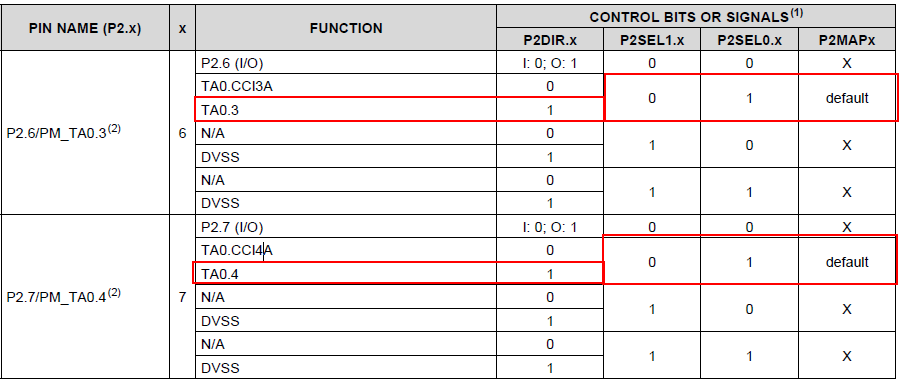
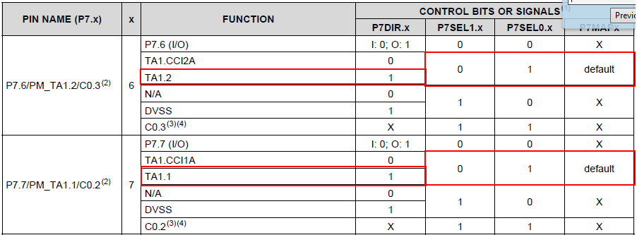
P7->Dir |= BIT6 | BIT7;
P7->SEL0 |= BIT6 | BIT7;
P7->SEL1 &|= ( BIT6 | BIT7);
which sets output to p7.6~7 set Ta1.1~2
trying to use pin 2.7
but fails to generate signal after these changes
P2->Dir |= BIT6 | BIT7;
P2->SEL0 |= BIT6 | BIT7;
P2->SEL1 &|= ( BIT6 | BIT7);
Thanks for all the help
Regards Paul

**Attention** This is a public forum