- Ask a related questionWhat is a related question?A related question is a question created from another question. When the related question is created, it will be automatically linked to the original question.
Part Number: MSP432P401R
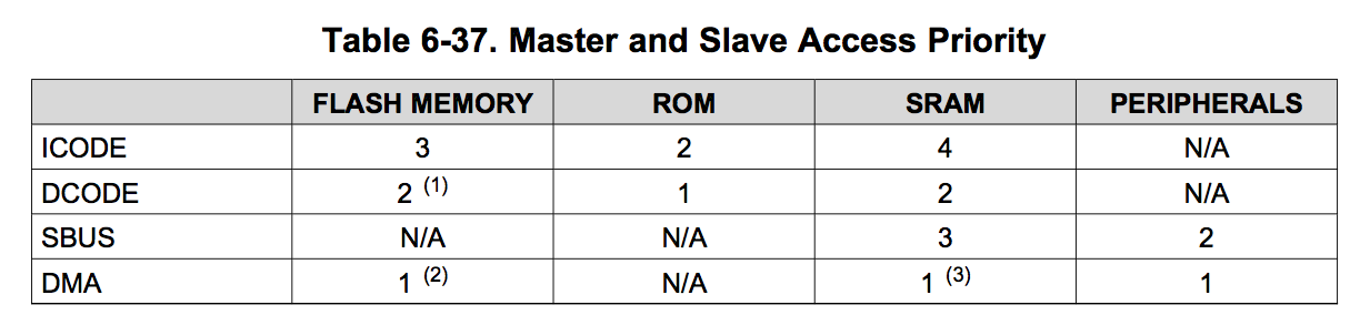
I've been through the data sheet and the TRM for the msp432p401r and can't find anything that talks about the DMA controllers impact on main cpu access to shared resources.
Can you please be more specific about how that works?
I'm assuming lacking other information that both the main cpu and the DMA AHB port have equal priority and so will simply round robin via arbitration.
does that yield effectively 50% sharing so the cpu data cycles will slow down an appropriate amount.


**Attention** This is a public forum