This thread has been locked.

If you have a related question, please click the "Ask a related question" button in the top right corner. The newly created question will be automatically linked to this question.

CCS/MSP430FR2633: FRAM example doesn't make sense (to me)

Part Number: MSP430FR2633
Other Parts Discussed in Thread: MSP430WARE

Tool/software: Code Composer Studio

I'm trying to understand how to store a value (unsigned long) in FRAM that, ideally, won't get erased when reprogramming the chip. 

First, the examples use a the PERSISTENT and NOINIT pragma, which seems straightforward. but do I need to worry about the address of those variables changing place in the future? For example, in this version of the firmware, I only store a single unsigned long. If I decided to store additional variables in the future, will the address for the original unsigned long stay the same? How do I find its address when using the NOINIT pragma?

Second, regarding NOINIT, I read SLAA628 - MSP430 FRAM Technolgoy - How To and Best Practices. In section 5.1 it states: (I added the emphasis) "Note that unlike PERSISTENT, variables declared as NOINIT do not get located in FRAM by the default linker command files, requiring a minor modification of the linker command file if such functionality is required." So... what needs to be modified in the link command file and how?

Third, looking at the msp430fr243x_framwrite.c example, I'm very confused. (I'm trying to link to it, but the editor keeps acting strangely. So, located at: TI Resource Explorer > Software > MSP430Ware > MS430FR2XX_4XX > MSP430FR2633 > Peripheral Examples > Register Level > msp430fr243x_framwrite.c.")

The description says you should disable interrupt while writing to the main FRAM. But then says "This code examples is using DFWP which wouldn't have dangerous." I have no clue what that statement means. The only thing that makes sense to me is that the example claims to be using DFWP.

In the code, FRAM-TEST_START is defined as 0x1800. Looking at the linker command file that corresponds with INFOA. Which has a comment that says "/* MSP430 INFO FRAM  Memory segments */." (Side note, what is an INFO FRAM memory segment?) If this example is writing to FRAM, why isn't the start address 0xC400?

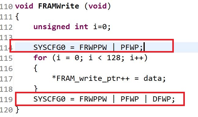
In the FRAMWrite() function it looks like SYSCFG0 unlocks PFWP not DFWP. I thought the clearly written description specifically stated this code was not doing anything with PFWP. So what is going on there?

Also, on the line the LED is toggled, the comment says "show 512 bytes." That doesn't make sense. The LED will toggle after 5120 bytes have been written. Or am I missing something?

Lastly, all of the marketing data I find says that FRAM doesn't have the life cycle issues of Flash. Yet this example clearly warns that "Running this example for extended periods will impact the FRAM endurance." Yikes! How dangerous is running this code?! What is defined as an "extended period?"

  • Hi James,

    Thanks for your post. I think you can find more detail description about your confusion in MSP430FR263x, MSP430FR253x Capacitive Touch Sensing Mixed-Signal Microcontrollers datasheet (Rev. B) and MSP430FR4xx and MSP430FR2xx Family User's Guide (Rev. H). For your questions:

    1. You can program variable at absolute address. Please see Placing Variables in Specific Memory Location - MSP430. And make sure your variables are referenced by the code or use .retain directive to avoid removal by linker. See this threads for more details ( https://e2e.ti.com/support/microcontrollers/msp430/f/166/t/707158 ).

    2. You can find the PERSISTENT and NOINIT section definition at lnk_msp430fr2633.cmd file. In the cmd file, you need delete the ".TI.noinit  : {} > RAM" and add code like below picture, which moves the .TI.noinit section from default RAM to FRAM.

    3. PFWP is for FRAM code memory protection to prevent any unwanted changed of code. DFWP is for FRAM information memory protection. Information memory usually is used to stored user's data. The data changed isn't more dangerous than code changed. Only when PFWP disable, you can write FRAM main memory. So, please enable PFWP as soon as the completion of write. But if interrupt happens at this time, it will expose FRAM at unprotected situation for a long time. Therefore, it's recommended to disable interrupt while code is writing to main FRAM.

    4. FRAM memory includes main memory and information memory. Please see MSP430FR263x, MSP430FR253x Capacitive Touch Sensing Mixed-Signal Microcontrollers datasheet (Rev. B) and MSP430FR4xx and MSP430FR2xx Family User's Guide (Rev. H) for more details. 

    5. You are right, "toggle LED after every 100 writes" is correct. The FRAM has 10^15 Write Cycle Endurance which means "no life cycle issues" in real applications. But if you only test FRAM endurance using this code example, it may exceed the 10^15 limitation.

    Best Regards,

    If my post helped solve your issue, please click on the  VERIFY ANSWER    button. 

    Winter,

    Search E2E! Your questions may already be answered! 

  • Winter Yu said:
    In the cmd file, you need delete the ".TI.noinit  : {} > RAM

    Yes. I figured this out. I am baffled why the application note I referenced does not include that 2 sentence explanation. Additionally, you forgot to mention that one also needs to disable the "Main memory only" erase option in the Debug tag of the project properties in CCS 8. Again, baffling why TI goes out of its way to hide these critical details. (It is, however, a very effective method to keep new engineers interested in the platform from adopting it.)

    Winter Yu said:
    PFWP is for FRAM code memory protection to prevent any unwanted changed of code. DFWP is for FRAM information memory protection

    This explanation does not answer my original question. I don't understand why the example has a cryptic statement about using DFWP but the code clearly references PFWP. WHY.? Other FRAM examples I have found use unlock DFWP as expected. Not the one I referenced. WHY. There must be a reason. What is that reason?

    Also, I am still looking for an explanation to FRAM write/life cycles. The example I referenced clearly warns about wearing out FRAM. I'm very concerned about this in my application. Please explain why the example warns about it. What is so critical that the example's author felt it necessary to include that warning?

  • Hi James, I can understand your frustration. I am the other thread that Winter shared, and am also working on managing the device memory.

    To your question about FRAM write cycles (and I may not fully understand your question), flash has a common write cycle limitation of 10^5 cycles (according to wikipedia), whereas this FRAM has an expected write cycle limitation of 10^15. I think this is where TI makes a reasonable claim that the life is "forever" for most applications. The risk comes when you specifically write code that just writes the same location over and over. Now, my back on the envelope calculation is that at 100k writes/second, it would still take 317 years to reach 10^15 writes, but it's likely the person who wrote the example is just covering their backside with that warning. :)

    I'll be digging into the difference between DFWP and PFWP myself to see if I can understand why I'm not initializing constants stored in INFO memory correctly. If I find something that seems useful, I'll post back here.

    Hope this helps,
    Paul
  • > whereas this FRAM has an expected write cycle limitation of 10^15
    Yes, I found various marketing information on the expected number of writes. However, the author for this example felt it was necessary to warn against this code being dangerous to the endurance of FRAM. That being the case, I need to know how dangerous this code is to run. (They did, after all, specifically use the word "dangerous.")
  • My questions will remain unanswered. This issue is not resolved, but I want to close out the question. I've decided to adopt a different platform.
  • Hi James,


    Thanks for using MSP430 devices and posting your questions. I and community member Paul Shepherd17 (thanks Paul) have already try to answer your questions. I’m sorry for your dissatisfaction with these answers. I'd like to make a summary and a further explain:


    1. How to store a value (unsigned long) in FRAM that, ideally, won't get erased when reprogramming the chip. 

    You have figured out this question according my answer.


    2. I am baffled why the application note I referenced does not include that 2 sentence explanation. Additionally, you forgot to mention that one also needs to disable the "Main memory only" erase option in the Debug tag of the project properties in CCS 8. Again, baffling why TI goes out of its way to hide these critical details. (It is, however, a very effective method to keep new engineers interested in the platform from adopting it.)

    Actually, the sentence “.TI.noint : {} > FRAM” makes “.TI.noinit” varibles locate into FRAM is described in the application note as below. Yes, I forgot to mention that one also needs to disable the "Main memory only" erase option. Thanks for your reminder.  Despite it’s a default setting, anyway, we should keep an eye on it.


    3. I don't understand why the example has a cryptic statement about using DFWP but the code clearly references PFWP. WHY.? Other FRAM examples I have found use unlock DFWP as expected. Not the one I referenced. WHY. There must be a reason. What is that reason?

    This code example demonstrates writing information memory(1800h-19FFh, protected DFWP), and remind the matters need attention if writing code memory(protected by PFWP). Actually, I didn’t see the thing makes you confused. When writing FRAM information, firstly the code disables DFWP by setting DFWP as 0 (SYSCFG0 = FRWPPW | PFWP) , and then enables DFWP. Anyway, using “SYSCFG0 &= ~DFWP” is clearer for understanding. Thanks for your feedback.


    4. Be confused about why the author for this example felt it was necessary to warn against this code being dangerous to the endurance of FRAM.

    Maybe "Dangerous" is not appropriate. It's just a reminder with caution. Anyway, thanks for your feedback. I will discuss with

    the author of this code example to make some improvement.

    For above questions and answers, about which one do you remain confused? Please feel free to post on E2E forum. Even if we do our best to provide good products, rich resources and easy to use ecosystem, there is still much room for improvement. It's man like you that makes TI become better and better.


    Best Regards,

    Winter Yu


**Attention** This is a public forum