This thread has been locked.

If you have a related question, please click the "Ask a related question" button in the top right corner. The newly created question will be automatically linked to this question.

MSP430F5529: PWM + Phase shift

Part Number: MSP430F5529

Hi,

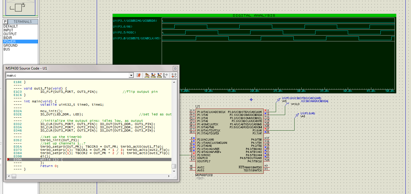
I am trying to generate 5 Square Waves shifted by 72 degrees w.r.t each other. I am using timer B in compare mode. My problem is that I am not able to initialize the initial state of the output pin. I want two of the signals to start from low and other three from high so that I can achieve the required phase shift.

Thanks

Nitish

  • Hi,

    initializing the initial state of the output pin is kind of tricky. You can do that by setting the OUTx Bit to the desired state but if you then go ahead and configue the output mode also the initial state will be overwritten after one clock to the initial state of the output mode.

    It might be an option to use two different output modes (Reset/Set and Set/Reset for example) but this then results in continuous inverted state switching. Another option could be to use the same output mode (with the same initial state) but adapt the CCRx values to account for the shift.

    Would any of those two options work for you? You'll find a more detailed description in the Timer_B User's Guide chapter.

    Best regards,
    Britta
  • Hi,

    I tried using the OUTx option but didn't notice any changes in my waveform. I can't use Reset/Set and Set/Reset as they won't give me 50% duty cycle and with CCRx values I can have a phase shifts of 0,72, 144 not more than that.

    Best Regards,
    Nitish
  • HI,

    your finding makes sense as it displays what I've explained: Your initial state would be overwritten by the default initial state of the output mode.

    I might have on proposal on how to solve your issue but this depends on your application so you have to tell me afterwards if this is even feasible for you:

    You can use TImer_B with 7 Capture/Compare Registers, CCR0 will set your PWM period, and you use the remaining CCRx (or rather 5 of those) to phase shift the different PWM signals and determine the duty cycle. I'd recommend to use the "Toggle" mode as output mode and up mode for the timer. However, what will be necessary is that you reconfigure each CCRx (for example CCR1 for the first PWM signal) after it generates the interrupt  and set it to the next value.

    Let's take an example:

    Your CCR0 is 2000 (PWM period).

    CCR1 is 200 at first, so when TBxR reaches 200 you'll receive an interrupt and OUT1 is set. Now you reconfigure CCR1 to 1200 so OUT1 will reset when TBxR reaches 1200.

    CCR2 is 300 at first, so when TBxR reaches 300 you'll receive an interrupt and OUT2 is set. Now you reconfigure CCR2 to 1300 so OUT2 will reset when TBxR reaches 1300.

    You can now adapt the shift and PWM period to your needs. In my example TBxR is cleared after reaching CCR0.

    Attention: You have to take care that there is enough time to actually do the reconfiguration of CCRx. This depends on the time in between the desired two edges and the clock you use for Timer_B.

    Let me know if this helps.

    Best regards,

    Britta

  • Thank you. I will try this once. I was thinking of putting up 2 "NOT" gates of the 36 degree and 72 degree waveform.

    Regards

    NItish

  • Thank you. I will try this once. I was thinking of putting up 2 "NOT" gates of the 36 degree and 72 degree waveform.

    Regards

    NItish

  • Can you send me some example. I tried to do it but the interrupts never been called. Also, now I have to do the configuration for phase shifted 75% duty cycle signals

    Regards

    Nitish
  • #include <msp430.h> 
    
    
    /**
     * main.c
     */
    
    void main(void)
    {
    
        WDTCTL = WDTPW + WDTHOLD;                 // Stop WDT
    
      /*P1DIR |= BIT0;                            // ACLK set out to pins
      P1SEL |= BIT0;
      P2DIR |= BIT2;                            // SMCLK set out to pins
      P2SEL |= BIT2;
      P7DIR |= BIT7;                            // MCLK set out to pins
      P7SEL |= BIT7;*/
    
      P5SEL |= BIT2+BIT3;                       // Port select XT2
      P5SEL |= BIT4+BIT5;                       // Port select XT1
    
      UCSCTL6 &= ~XT2OFF;                       // Set XT2 On
      UCSCTL6 &= ~XT1OFF;                       // Set XT1 On
      UCSCTL6 |= XCAP_3;                        // Internal load cap
    
      UCSCTL1 = DCORSEL_5;
      UCSCTL2 = FLLD_1 + (218);
    
      // XT1 is by default on as it is used default reference for the FLL - internal load caps?
      // Loop until XT1,XT2 & DCO stabilizes
      do
      {
        UCSCTL7 &= ~(XT2OFFG + XT1LFOFFG + DCOFFG);
                                                // Clear XT2,XT1,DCO fault flags
        SFRIFG1 &= ~OFIFG;                      // Clear fault flags
      }while (SFRIFG1&OFIFG);                   // Test oscillator fault flag
    
      UCSCTL6 &= ~XT2DRIVE0;                    // Decrease XT2 Drive according to
                                                // expected frequency
      UCSCTL4 |= SELA_0 + SELS_5;               // Select SMCLK, ACLK source and DCO source
    
            P5SEL |= 0x80;
            P5DIR |= 0x80;
          //  P5OUT |= BIT7;
            P7SEL |= 0x50;
            P7DIR |= 0xFF;
            //P7OUT |= 0x50;
            P3SEL |= 0x60;
            P3DIR |= 0xFF;
            //P3OUT &= ~(BIT4+BIT5);


            TB0CCR0 = 89;
    
            //TB0CCTL1 |= BIT2;
          // TB0CCTL2 |= BIT2;
          // TB0CCTL4 |= BIT2;
            TB0CCTL1 = OUTMOD_7;
            TB0CCR1 = 68;
    
            TB0CCTL2 = OUTMOD_4 + CCIE;
            TB0CCR2 = 18;
    
            TB0CCTL4 = OUTMOD_4 + CCIE;
            TB0CCR4 = 14;
    
            TB0CCTL5 = OUTMOD_4 + CCIE;
            TB0CCR5 = 32;
    
            TB0CCTL6 = OUTMOD_4 + CCIE;
            TB0CCR6 = 50;
    
            TB0CTL = TBSSEL_2 + MC_1 + TBCLR + TAIE;
    
            __bis_SR_register(LPM0_bits + GIE);


    while (1);


    }
    
    
    #if defined(__TI_COMPILER_VERSION__) || defined(__IAR_SYSTEMS_ICC__)
    #pragma vector=TIMERB0_VECTOR
    __interrupt void TIMERB0_ISR (void)
    #elif defined(__GNUC__)
    void __attribute__ ((interrupt(TIMERB0_VECTOR))) TIMERB0_ISR (void)
    #else
    #error Compiler not supported!
    #endif
    {
        switch( __even_in_range(TB0IV,12) )
        {
        case 4:
            if (TB0CCR2 == 18)
            {
                TB0CCR2 = 86;
            }
            else
            {
                TB0CCR2 = 18;
            }
            break;
        case 8:
               if (TB0CCR4 == 14)
               {
                   TB0CCR4 = 36;
               }
               else
               {
                   TB0CCR4 = 14;
               }
               break;
        case 10:
               if (TB0CCR5 == 32)
               {
                   TB0CCR5 = 54;
               }
               else
               {
                   TB0CCR5 = 32;
               }
               break;
        case 12:
               if (TB0CCR6 == 50)
               {
                   TB0CCR6 = 72;
               }
               else
               {
                   TB0CCR6 = 50;
               }
               break;
        default:
            break;
        }
    
    }


    //the interrupts doesn't seem to work. Can you tell me where am I going wrong?
    

  • much simpler than that: in this case, 3 channel output, each 60 degrees off of each other.

  • Hi Nitish,

    did you have a look at what Danny provided you with?
    Are there any remaining open items? In case your questions with regards to the interrupts is still open I'd advise you to have a look at the code examples we provide as part of the TI Resource Explorer.

    Please let me know what your current status is.

    Thanks and best regards,
    Britta

**Attention** This is a public forum