This thread has been locked.

If you have a related question, please click the "Ask a related question" button in the top right corner. The newly created question will be automatically linked to this question.

CCS/MSP432P401R: How to connect the analog input to MSP432P401R Launchpad in differential mode?

Part Number: MSP432P401R

Tool/software: Code Composer Studio

Hi,

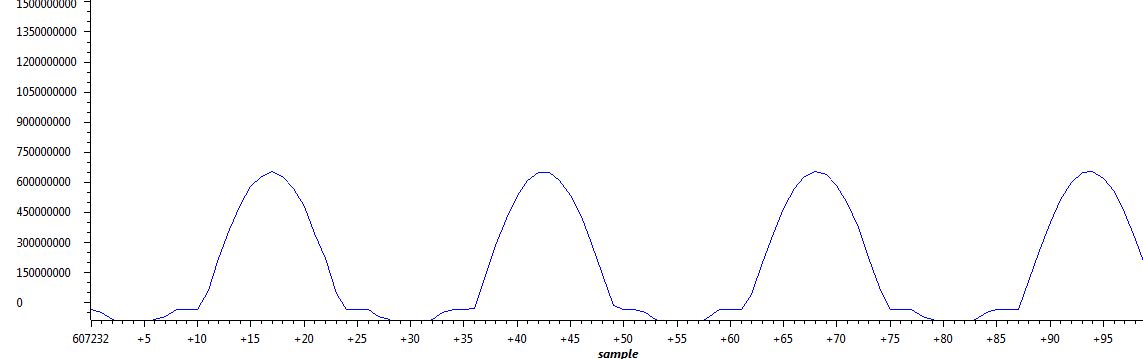
I am trying to use 14 bit ADC of MSP432P401R Launchpad in differential mode. Could you tell me the right way of connecting the analog input to the Launchpad? Right now, I am connecting the +ve terminal of the input to pin "P4.3" and the negative terminal of the input to "P4.2". Is this connection correct?

Mohammad Arifur Rahman

  • Hello,

    P4.3 is also A10 and P4.2 is A11.  You are correct, that in differential mode this is channel A10 as defined in the TRM (A10 is the positive and A11 the negative).

    Regards,
    Chris

  • Thanks for your reply. In the differential mode, I am using a 1 V (P-P), 20 Hz sinusoidal signal from a signal generator as an input. The ADC result found in CCS is given below:

    This result I got when I am using 500 mV offset for the 1 V (P-P) input:-

    But when I am using 0 mV offset for this 1 V (P-P) input signal, I got the following ADC result:

    Do I have to use an external offset if there is negative portion in my analog input voltage?

    I am using the following code for configuring my ADC.

    /* Initializing ADC (MCLK/1/1) */
    ADC14_enableModule();
    ADC14_initModule(ADC_CLOCKSOURCE_MCLK, ADC_PREDIVIDER_1, ADC_DIVIDER_1, 0);

    ADC14_setSampleHoldTrigger(ADC_TRIGGER_SOURCE1, false);

    /* Configuring GPIOs (4.3 A10) */
    GPIO_setAsPeripheralModuleFunctionInputPin(GPIO_PORT_P4, GPIO_PIN3,
    GPIO_TERTIARY_MODULE_FUNCTION);

    /* Configuring ADC Memory */
    ADC14_configureSingleSampleMode(ADC_MEM0, true);
    ADC14_configureConversionMemory(ADC_MEM0, ADC_VREFPOS_AVCC_VREFNEG_VSS,
    ADC_INPUT_A10, true);//false

    /* Set ADC result format to signed binary */
    ADC14_setResultFormat(ADC_SIGNED_BINARY);

    Mohammad Arifur Rahman

  • Do not apply negative voltages to the device.  You can risk damaging the part.  

    The differential voltage is relative to the differential pair.  You can put the negative input to the offset voltage and then connect the positive to your input source.  Both signals, however, must be within the recommended operating conditions of the device.

    Chris

  • Hi Chris,

    Thanks for your reply. I was also using the offset from the signal generator. But for the application, do I have to make a circuit for giving the offset for the negative part of the voltage?


    Mohammad Arifur Rahman
  • I am not sure what you mean, but the voltage on any pin of the chip must be from between -0.3 to Vcc + 0.3 V, relative to Vss. Basically, both voltages must be positive relative to Vss.
  • Hello,

    Q: But for the application, do I have to make a circuit for giving the offset for the negative part of the voltage?
    YES, you have.

    Your 1st picture shows 1.3 V (P-P) , if you have applied right scaling.
    On P4.2 you have applied -0.35V out of absolute maximum ratings.
    Hope your ADC input pin has survived.
  • Thanks for your important suggestions.


    Mohammad Arifur Rahman
  • You are welcome.

    Having a generator with an output impedance @ 50 Ohm you could stress PIN protecting diodes with 5-6 and up to 7 mA for a relatively long time @ 20 Hz.

**Attention** This is a public forum