This thread has been locked.

If you have a related question, please click the "Ask a related question" button in the top right corner. The newly created question will be automatically linked to this question.

CCS/MSP430I2021: SD24 offset error compensation

Part Number: MSP430I2021

Tool/software: Code Composer Studio

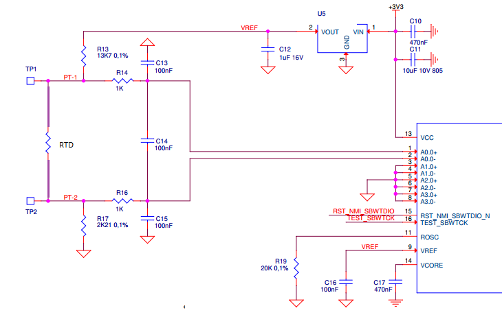
On my custom board I use SD24 to acquire a differential signal on A0.0+ and A0.0- inputs. The A1.0+ and A1.0- inputs are both tied to GND. VCC = 3.3V.

I use a nominal 1.25V external reference voltage to feed the input signal and the VREF input of SD24 (ratiometric acquisition). The measured reference voltage is 1.266V.

SD24 is initialized as follows:

	SD24CTL = 0;	// External ref
	SD24CCTL0 = SD24DF | SD24IE;	// 2-compl. data format, continuous conv, enable interrupt
	SD24INCTL0 = SD24GAIN_8;	// input A0, Gain=8, Interrupt on 4th sample

When I start conversions with

    SD24CCTL0 |= SD24SC;	// Set bit to start conversion

I count 8 conversion interrupt; in each conversion interrupt I accumulate the (short int)SD24MEM0 value to make an average conversion value at the end of the 8th interrupt, when I stop conversions with 

	SD24CCTL0 &= ~SD24SC;		// clear bit to stop conversion

I know from the MSP430I2021 datasheet the SD24 gain tolerance (±1%) and the SD24 max offset error (2÷4 mV) in the external reference case with SD24OSRx=256. I suppose a 2.5mV offset error with gain 8. The 2.5mV offset error would give (2.5mV * 8 * 32767)/1.266V = 534 ADC offset value added to every (short int)SD24MEM0 conversion result. Indeed, with a given input signal on A0 input I see conversion values differ from the expected ones by 500-650 ADC counts.

Now, in order to compensate that SD24 offset error I tried to acquire the GND signal tied to A1 input channel with the same A0 input channel configuration. The (short int)SD24MEM1 conversion result should be (more or less) the SD24 offset error to be subtracted from the (short int)SD24MEM0 conversion results of the A0 input signal.

But in this way I get 39 as measured SD24 offset error. Also, I get 82 as conversion result with A0 signal at 0V (without compensation).

Could you please explain the reason why? Where am I wrong?

  • Hi, Vagniluca, 

    Do you have tried the gain setting to x1 and what is the conversion result for A0 and A1? 

    Best regards, 

    Lixin 

  • Hi Lixin,

    On my board I have external voltage reference measured at 1.266V.

    I repeated my test measures with GAIN = 1 and with GAIN = 8.

    • GAIN = 1

    SD24 offset error on A1 = 0

    A0 Vin (V) ADC result

    Expected

    ADC result

    Difference
    0 3 0 3
    0,0668 1770 1728 42
    0,0733 1940 1897 43
    0,0798 2112 2065 47

    • GAIN = 8

    SD24 offset error on A1 = 39

    A0 Vin (V) ADC result

    Expected

    ADC result

    Difference
    0 86 0 86
    0,0668 14613 13831 782
    0,0733 16010 15177 833
    0,0798 17424 16523 901

    All the result values above are not compensated with the SD24 offset error measured on A1.

    All the results are the average values on 8 consecutive conversions.

    I do not undestand why the difference values are so far from the one I get with 0V input, especially with GAIN = 1.

    Also, although all the conversions are made with the A0 Vin signal already settled, more than the first 3 conversion results need to be discarded, because the result value increases at each new conversion and then is settled. This is true especially for GAIN = 8. Then I have to discard the first 13 conversion results before starting the average on surely settled result values.

    Best Regards

    Alessandro

  • Hi, Alessandro, 

    I don't see the problem for the software configuration. You discard first 13 conversion data and make average for 8 conversion results. 

    1. Could you help to check if the the external Voltage reference voltage is stable or not? Is there any de-coupling capacitor on VREF pin?

    2. Do you have tried internal voltage reference and see difference? Datasheet recommend capacitor on VREF pin is 100nF when using internal voltage reference. Please make sure the board has the capacitor. 

    3. Another thing needs to be checked: datasheet recommend to connect unused pin to AVSS. Could you help to check it? 

    4. When ADC conversion, it is better no GPIO toggling and no high frequency clock toggling because this will cause noise on ground. Could you help to check this? 

    Best Regards, 

    Lixin 

  • Hi Lixin,

    I don't see the problem for the software configuration. You discard first 13 conversion data and make average for 8 conversion results. 

    OK, but on the MSP430I20xx Family User's Guide I see that just 4 conversions (digital filter settle time) are needed to have an ADC result stable in any case. Maybe, this is true only for GAIN = 1 ?

    1. Could you help to check if the the external Voltage reference voltage is stable or not? Is there any de-coupling capacitor on VREF pin?

    2. Do you have tried internal voltage reference and see difference? Datasheet recommend capacitor on VREF pin is 100nF when using internal voltage reference. Please make sure the board has the capacitor. 

    Yes, the external voltage reference is 1.266V stable. I measure the same voltage on the VREF pin, which is de-coupled with a 100nF capacitor.

    I cannot try internal voltage reference: I should trim the net on the VREF pin on my board.

    3. Another thing needs to be checked: datasheet recommend to connect unused pin to AVSS. Could you help to check it? 

    I use only A0 input in differential mode with the following circuit:

    A1, A2 and A3 inputs are all tied to AVSS.

    4. When ADC conversion, it is better no GPIO toggling and no high frequency clock toggling because this will cause noise on ground. Could you help to check this? 

    On my board I blink a led with Ton=Toff=1s. I get the same results with no led blinking.

    I use MCLK = DCO/2 = 8.192MHz, SMCLK = DCO/4 = 4.096MHz, External Resistor as clocks configuration.

    I get the ADC conversion results through my debugger, stopping the firmware with a breakpoint at the end of each average calculation. I use Spy-by-Wire (2-wire JTAG) program/debug interface with my MSP-FET430UIF v1.4a. Could the debugger presence affect the ADC conversion results?

    Best Regards

    Alessandro

  • Hi, Alessandro, 

    I mean it is fine that You discard first 13 conversion data and make average for 8 conversion results. 

    Sorry, I cannot see the circuit you attached. It is showed as a small symbol. If the A1, A2, and A3 are tied to AVSS, it should be ok. But it seems the A0 and A1 are not connected to the same GND point. Do you have measure the voltage difference for A0 and A1 when setting them to GND? 

    I am not sure if the debugger is the noise source. But it is valuable the check the free running result without debugger connected if there is no other suspected point. 

    In addition, could you let me know how the offset error 39 was achieved? You attached following description for Gain=8. 

    • GAIN = 8

    SD24 offset error on A1 = 39

    Regards, 

    Lixin 

  • Hi Lixin,

    I try to attach my complete analog input circuit.

    So, you can see A0 is the used differential input, A1 input is tied to AVSS.

    SD24 offset error on A1 was achieved converting A1 input with the same gain and average procedure used on A0 input. Because A1 is tied to AVSS, I suppose (am I right?) A1 conversion value could be the compensation offset value to be subtracted from every A0 conversion value. But when I set Vin = 0V (i.e. RTD = 0 Ohm) on A0 input, I read a much greater value then the compensation offeset value.

    Best Regards,

    Alessandro

  • Hi, Alessandro, 

    Thanks for the schematic attached. 

    RTD=0-ohm cannot be regarded same as A1 input which is connected to AVSS directly. You can cut off the components on A0 circuit and connect A0 to the same grounding point AVSS as A1 input. Then do the ADC conversion again to check the difference between A0 and A1 channels. 

    For your circuit, A0 input is connected to the VREF through resistors and capacitors. For offset calibration, the voltage between A0+ and A0- should be 0. It is recommended to remove R13 and R17, short RTD, R14, and R16. 

    I don't know what is the function for R13 and R17. It seems to provide voltage to external circuit. I am not sure if they will impact the offset result. If the resistors will work in normal application, maybe they need to be reserved for the offset calibration, i.e. RTD=0-ohm as your mentioned method. 

    If you want to use A1 conversion result as the offset compensation value, it is recommended to connect the same input circuits as A0 except the RTD is 0-ohm. 

    Best regards, 

    Lixin 

  • Hi, Alessandro, .

    Do you have any update for this? 

    If my comment is helpful to resolve your questions, please click on the This resolved my issue  button to close this thread.  

    Regards, 

    Lixin

**Attention** This is a public forum