This thread has been locked.

If you have a related question, please click the "Ask a related question" button in the top right corner. The newly created question will be automatically linked to this question.

CCS/MSP430F6638: MSP430F6638 timer and ADC interrupt

Part Number: MSP430F6638

Tool/software: Code Composer Studio

Hello,

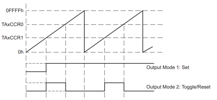
I am using the ADC12 of the MSP430F6638. I need a 100Hz sample rate ADC, and the 100Hz is generated by timer. Otherwords, a 100Hz signal is generated by timer to trigger the ADC's sample and conversion. I am using the up mode for the timer and the toggle and reset mode.

I would like in my program at each rising edge of the toggle and reset signal and so the timer signal to have an interrupt where I could enable and start the ADC12 conversion. I'm not sure at all if this seems to be correct but here is what I tried :

*******************************   Configuring 100 Hz timer signal  ************************************

P1SEL|=BIT1;                                                        //SELECT P1.1 AS TA0 and not I/O where we set the period of the timer signal
P1DIR|=BIT1;
P1SEL|=BIT2;                                                       //SELECT P1.2 AS TA0 output and not I/O where we set the duty cycle of the timer signal
P1DIR|=BIT2;
TA0CCR0 = 320 - 1;                                            // 100hz sampling frequency
TA0CCR1 = 295;                                                 // duty cycle not important it's the period which is important
TA0CCTL1 = OUTMOD_2;                                // out mode 2
TA0CTL = TASSEL_1 + TACLR+ MC_1;          // ACLK, up mode

TA0CCTL1|= CCIE;                                         // enable interrupt

1) Here should I enable an interrupt on the P1.2 pin where we set the duty cycle of the signal or on the P1.1 pin where we set the period of the signal ? In other words it's TA0CCTL1|= CCIE or TA0CCTL0|= CCIE ?

*************  Interrupt routine  **********************

#pragma vector=TIMER0_A0_VECTOR

__interrupt void TIMER0_CCR0_ISR(void){

ADC12CTL0 |= ADC12ENC|ADC12SC; // enable and start conversion
}

2) Is this the correct way to write the interrupt routine ? Is it right as it's written or it's __interrupt void TIMER0_CCR1_ISR  (CCR0 or CCR1) ? Is it TIMER0_A0 considering my configuration of timer above ? Do I have to clear the interrupt flag in the interrupt or it is cleared automaticaly ?

3) Also i saw in many examples this _BIS_SR(GIE). Is this important to use ? I mean with the code i have written above am I going to enable and start a new conversion each rising edge of my timer signal or there is some mistakes ?

4) My last question is also about interrupt but this time for ADC12. I also need in my program to have an interrupt each time a conversion is completed. To do this I wrote the interrupt routine where I set a variable equal to 1 so I can read outside the interrupt the ADC12MEM5 (i use ADC5) by testing in the main program if this variable is equal to 1 and if yes I read the ADC12MEM5 register and the variable become 0. But also here i'm not sure at all if it's correct and if I have to use the _BIS_SR(GIE); command. Here is my code.

************************* ADC12 CONFIGURATION ********************************

P6SEL|=BIT5;                                                                                                                //SELECT P6.5 AS ADC and not I/O
ADC12CTL0 &= ~ADC12ENC;                                                                                      // ADC12 disabled
ADC12CTL0 = ADC12REFON + ADC12ON + ADC12REF2_5V + ADC12SHT0_2;    // Sample time 16, around 16/4.8MHz = 3.3us, reference 2.5 V, reference on and ADC12 on
ADC12CTL1 = ADC12SHP + ADC12SHS_1 + ADC12DIV1;                                     // enable sample timer, ADC clock from MODCLK, trigger source 1 timer
ADC12MCTL6 = ADC12SREF_1 + ADC12INCH_5;                                                 //  ADC5 
ADC12IE = ADC12IE0;

Here I am not sure at all about the interrupt enable command since it talks about a specific bit whereas in my program i need an interrupt not on a specific bit but when a conversion is completed (when the 12 bits word is ready to be read).

****************************** INTERRUPT ROUTINE *****************************************

#pragma vector = ADC12_VECTOR
__interrupt void adc12_ISR(void)
{

write_mem = 1;
}

Since I am using the ADC5 (P6.5 pin of MSP430F6638) should number 5 appear somewhere in the interrupt name or as it's written it's correct ? 

*****************  MAIN PROGRAM ************************

if (write_mem == 1)

{

write_mem = 0;

converted_value = ADC12MEM5;

}

Since the flag is automaticaly cleared when we access the ADC12MEMX register no need to clear the flag in the interrupt, right ?

Thank you.

Best regards,

Mike

  • With SHS=1 (TA0.1 trigger) there's no need for the timer interrupt at all -- the timer will trigger the ADC directly and the ADC interrupt will tell you when it's done. You don't even need to configure the pin unless you want to for other reasons.

    But to answer your questions:

    1) TIMER0_A0_VECTOR services Only the CCTL0:CCIFG interrupt. All the others are serviced by TIMER0_A1_VECTOR.

    2) The ADC12_VECTOR services any/all of the ADC IFGs. The ISR has to know which MEMx register(s) are relevant.

    3) Yes, reading the MEMx register clears that IFG.

    4) _BIS_SR(GIE) (aka __enable_interrupt()) needs to be done at some time or another (normally once initialization is done, then leave it on forever) so that your program can process interrupts.

    5) ADC12IE0 refers to MEM0/MCTL0, not MEM6/MCTL6. You need to change one of these to match the other.

    [Edit: Future pitfall in (3): With SHS>0 you need to toggle ENC (low then high) in the ISR or the ADC will stall. [Ref: User Guide (SLAU208Q) Fig 28-7, that arrow on the right]]

  • Hi Bruce,

    Thank you for your response. So considering point by point :

    1) According to you, if I want at each rising edge of my 100 Hz signal to enable and start a conversion, I don't need a timer interrupt since the timer will trigger the ADC directly, right ? Then where and when in my program should I set the command ADC12CTL0 |= ADC12ENC|ADC12SC; to enable and start a conversion ? I mean the timer triggers the ADC but how should the program know that at each rising edge we want to enable and start a conversion ?

    "With SHS>0 you need to toggle ENC (low then high) in the ISR or the ADC will stall". In which ISR ? The ADC one ? Since the timer interrupt is no longer necessary where to enable and start a conversion ?

    2)  "The ADC12_VECTOR services any/all of the ADC IFGs. The ISR has to know which MEMx register(s) are relevant."


    I am using the A5 of port 6 of the MSP430F6638 (P6.5). Where in the definition of the __interrupt void adc12_ISR(void) should I precise that I am using the A5 of port 6 ? 

    3) _BIS_SR(GIE) should this command be written once in the void main() of the program ? And by writting it like this are we enabling interrupt just for a specific peripheral or all of them ?

    4)  So know considering point 4 and 5 of your last post the code should look like this :

    _BIS_SR(GIE);   // to enable interrupt 

    *******************************   Configuring 100 Hz timer signal  ************************************

    P1SEL|=BIT1;                                                        //SELECT P1.1 AS TA0 and not I/O where we set the period of the timer signal
    P1DIR|=BIT1;
    P1SEL|=BIT2;                                                       //SELECT P1.2 AS TA0 output and not I/O where we set the duty cycle of the timer signal
    P1DIR|=BIT2;
    TA0CCR0 = 320 - 1;                                            // 100hz sampling frequency
    TA0CCR1 = 295;                                                 // duty cycle not important it's the period which is important
    TA0CCTL1 = OUTMOD_2;                                // out mode 2
    TA0CTL = TASSEL_1 + TACLR+ MC_1;          // ACLK, up mode

    ************************* ADC12 CONFIGURATION ********************************

    P6SEL|=BIT5;                                                                                                                //SELECT P6.5 AS ADC and not I/O
    ADC12CTL0 &= ~ADC12ENC;                                                                                      // ADC12 disabled
    ADC12CTL0 = ADC12REFON + ADC12ON + ADC12REF2_5V + ADC12SHT0_2;    // Sample time 16, around 16/4.8MHz = 3.3us, reference 2.5 V, reference on and ADC12 on
    ADC12CTL1 = ADC12SHP + ADC12SHS_1 + ADC12DIV1;                                     // enable sample timer, ADC clock from MODCLK, trigger source 1 timer
    ADC12MCTL6 = ADC12SREF_1 + ADC12INCH_5;                                                 //  ADC5 
    ADC12IE = ADC12IE5;                                                                                              

    Here for enabling the interrupt, it's ADC12IE5 and not ADC12IE6 as you mentioned, since I am using A5 of P6.5 pin as ADC12, right ? And by writing ADC12IE = ADC12IE5; is it enough to get with ISR definition below a interrupt each time a conversion is completed ?

    ****************************** INTERRUPT ROUTINE *****************************************

    #pragma vector = ADC12_VECTOR
    __interrupt void adc12_ISR(void)       // where to precise in the ISR that it's the A5 ???
    {

    write_mem = 1;
    }

    Thank you.

    Regards,

    Mike

  • Hey Mike,

    Bruce provided some great advice above and is correct about the timer already being connected to the ADC so the interrupt and pin configurations do not have to be used. 

    Also, the GIE = Global Interrupt Enable.  This has to be set to enable any interrupts in the MCU.  This can be done the two ways that Bruce mentioned.  

    Finally, I couldn't find any examples that show the ADC triggered by the timer, but I wanted to make sure you were aware of all the examples on TI Resource Explorer: http://dev.ti.com/tirex/explore/node?node=AKdBlqImUz6tvVbABDpt4g__IOGqZri__LATEST 

    Thanks,

    JD

  • 1) SC is only required with SHS=0. With SHS=1 the timer rising edge triggers the conversion. Toggle ENC inside the ADC ISR.

    2) You told the ADC about A5 by storing it in the MCTL register. Beyond that the code is only concerned with MEM (and implicitly MCTL) registers.

    > ADC12IE = ADC12IE5;     

    >> 5) ADC12IE0 refers to MEM0/MCTL0, not MEM6/MCTL6 [...and not to A0. By implication ADC12IE5 refers to MEM5/MCTL5, not A5.]

    It doesn't really matter which MEM/MCTL pair you choose, but if it's not MEM0/MCTL0 you also need to set CSTARTADD. I suggest you use MEM0/MCTL0/IE0 for simplicity.


  • Hi Bruce,

    Thank you for your response.

    1) "SC is only required with SHS=0. With SHS=1 the timer rising edge triggers the conversion. Toggle ENC inside the ADC ISR."


    Ok so here since SHS=1 I don't need to set the ADC12SC bit, so I just need to set the ADC12ENC bit. But you said in the ADC ISR. I am a little bit confused about which ADC ISR, because if we write this ;

    #pragma vector = ADC12_VECTOR
    __interrupt void adc12_ISR(void)       
    {

    ADC12CTL0 |= ADC12ENC;
    }

    , then what would be the inetrrupt routine that will indicate that a conversion is completed, where I could set my variable "write_mem =1;" to indicate in my program that a new value is availabe to be read from ADCMEMX ? I mean according to me we should have an interrupt where we enable the conversion and another one where which indicate that a conversion is completed, because I need in my program to know when a new converted value is available so I can only read and save new values and not old ones or read and save several times the same old value, since the MCU is much more faster than the 100 Hz sampling rate. This is the reason why I use the write_mem variable, since I need it to be set to 1 when a conversion is completed and to remain zero when it's not completed yet.

    2) "You told the ADC about A5 by storing it in the MCTL register. Beyond that the code is only concerned with MEM (and implicitly MCTL) registers.>> 5) ADC12IE0 refers to MEM0/MCTL0, not MEM6/MCTL6 [...and not to A0. By implication ADC12IE5 refers to MEM5/MCTL5, not A5.]"

    Ok so instead of ADC12IE = ADC12IE5; we should have ADC12IE = ADC12IE0. Ok it's clearer now. So even if i use A5 it doesn't matter and I can use ADCMEM0 to get the converted data, right ? Then what are the other ADCMEMX (ADCMEM1, ADCMEM2,...) for ? 

    3) Joining the first question, if we have two interrupt (one for enabling and the other to know if a conversion is completed), how to configure the ADC12IE field ? I mean how to deal with the fact that we need (or maybe not) 2 interrupts and the ADC12IE field configuration ? 

    4) Finally, should I write this command _BIS_SR(GIE) only once in the main void of my program ? 

    Thank you very much.

    Regards,

    Mike

  • 1) I'm going to change my suggestion: Right now you're using CONSEQ=0 and MSC=0. If you use CONSEQ=2 with MSC=0 you don't need to toggle ENC at all -- just set it at the beginning and leave it on. [Ref User Guide  (SLAU208Q) Fig 28-9 -- note the difference in the almost-rightmost arrow]. If you decide to work with more than one channel, this trick doesn't work, but for one channel it's fine.

    2) You can configure other MEMx/MCTLx for other input channels.

    4) Set GIE once initialization is done, then leave it on forever.

  • Hi Bruce,

    Ok it's a little bit clearer now. I am using the ADC to convert some data from an analog pressure sensor, and I would like to write a function ADC_ON() where I turn on and enable the ADC and a function ADC_OFF() to turn off the adc. So would you advise me to use CONSEQ=2 or CONSEQ=0 ? In my point of view since I have to convert some data from the pressure sensor during a certain time (typically 20 seconds for each measure, so  only during these 20 s I need the ADC_ON then I need the ADC_OFF all the way long) I would say CONSEQ=2 seems to be better, I don't know if you're joining my opinion.

    But I'm sorry, I still don't understand what I have to do to get an interrupt each time a conversion is completed. I mean how to know when a conversion is completed ? And if use CONSEQ=2 and set ENC at the beginning, then what about ADC12SC ? Where to set it ? I mean know it's clear for ENC but not really for ADC12SC, how to know when a conversion is completed and if an interrupt (ADC ISR) is required to let us know when a conversion is completed.

    Thank you very much.

    Regards,

    Mike

  • With SHS>0 (your case) you never use ADC12SC. The timer pulse (rising edge) completely subsumes that function.

    Since you're using MCTL0/MEM0 (with INCH_5) and IE0, every time the ADC finishes a conversion your adc12_ISR() will be called. When you get there you could check to see if IFG0 is set, but since IE0 is the only interrupt source you've enabled, you can reasonably assume that IFG0 is what triggered it. Reading MEM0 will clear IFG0, then you can return. adc12_ISR() will be called again when the next conversion (triggered by the next timer pulse) is complete.

    If you want to suspend the ADC sampling, the simplest way is to halt the timer. Setting MC=0 will "freeze" the timer in its current state, so the ADC won't see any (new) pulses. When you want to resume, set MC=1 again. This would work for either CONSEQ=0 or 2.

  • Hi Bruce,

    So if I did understand we should have something like this for the code :

    1) 

    int main(void)
    {

                                              *****************  ADC and timer configuration *********************************************************

     _BIS_SR(GIE);

    P6SEL|=BIT5;                                                                                                                                        //SELECT P6.5 AS ADC and not I/O
    ADC12CTL0 &= ~ADC12ENC;                                                                                                             // ADC12 disabled
    ADC12CTL0 = ADC12REFON + ADC12ON + ADC12REF2_5V + ADC12SHT0_2 + ADC12ENC;   // Sample time 16, around 16/4.8MHz = 3.3us, reference 2.5 V, reference on, ADC12 on and enable conversion

    ADC12CTL1 = ADC12SHP + ADC12SHS_1 + ADC12DIV1 + ADC12CONSEQ_2;                      // enable sample timer, ADC clock from MODCLK, trigger source 1 timer and CONSEQ =2 so we set ENC juts once. 

    ADC12MCTL0 = ADC12SREF_1 + ADC12INCH_5;
    ADC12IE = ADC12IE0; 

    P1SEL|=BIT1;                                                       //SELECT P1.1 AS TA0 and not I/O
    P1DIR|=BIT1;
    P1SEL|=BIT2;                                                      //SELECT P1.2 AS TA0 output and not I/O
    P1DIR|=BIT2;
    TA0CCR0 = 320 - 1;                                          // 100hz sampling frequency
    TA0CCR1 = 295;                                               // duty cycle not important it's the period that is important
    TA0CCTL1 = OUTMOD_2;                               // out mode 2
    TA0CTL = TASSEL_1 + TACLR+ MC_1;         // ACLK, up mode
    TA0CCTL1|= CCIE;                                        // enable interrupt

    }

    So for the configuration it seems to be correct, right ? I just have a doubt about the last line. Do I have to enable the interrupt for the timer that triggers the ADC or we just need the ADC interrupt ? 

    2) Now since i need in a while(1) loop to turn on and off the ADC we should have something like this, right ?

    while(1)

    {

    TA0CTL&=~MC_0; // ADC_OFF

    TA0CTL|=MC_1; // ADC_ON

    }

    Which is better to turn off the ADC : halt the timer by setting MC_0 or disable the ADC12ON field of the ADC ? 

    3) Finally I would like to be sure about the proper way to call the adc12 isr :

    #pragma vector = ADC12_VECTOR
    __interrupt void adc12_ISR(void)
    {
    write_mem = 1;

    }

    Do I need to add something to precise that I use the A5 chanel or is it correct like this ?

    Thank you very much,

    Regards,

    Mike

  • 1) ADC12CTL0 = ADC12REFON + ADC12ON + ADC12REF2_5V + ADC12SHT0_2 + ADC12ENC;  

    Set ADC12ENC last, (typically) as a separate step at the end of ADC initialization. Once it's set, some fields can't be changed.

    > TA0CCTL1|= CCIE;   

    Don't enable the timer interrupt unless you plan to do something with it. If you set the CCIE you'll need an ISR for it.

    2) TA0CTL&=~MC_0; // ADC_OFF

    MC_0 doesn't really do what you want here. Since you know MC=1, you could do:

    > TA0CTL&=~MC_1; // ADC_OFF

    3) In the ADC ISR you need to clear IFG0 by reading MEM0, so add something like

    > adc_value = ADC12MEM0;   // Fetch conversion result

    -------------------

    In that while(1) loop in (2), I would expect to see some code deciding when to turn the timer off and on. As coded, this will toggle the timer so fast it won't be detectable, except that the timer will appear to run kind of slow.

  • Hi Bruce,

    So basically I am trying to develop a blood pressure monitor. So during the deflation of the cuff I am collecting data from an analog pressure sensor, and converting this data thanks to the ADC. So I just need to turn on the ADC during the deflation of the cuff and once the deflation is complete I don't need to collect and convert data anymore until the next measure, that's why I need here to turn off the ADC. So in the while(1) loop I would have something like this :

    while(1)

    {

    if (step_2 == 1)        // step just a variable to test if step_1 is complete
    ADC_ON();             // didn't put it in the while below because just need to turn it once then turn it off when the deflation will be finished (when val_threshold will be < threshold) 

    while (val_threshold > threshold)   // comparing val threshold to the threshold pressure during deflation
    {
    valve_ON();
    if (write_mem == 1)    // this test allow us to know that a new value has been converted since write_mem is set to 1 when ADC12_ISR is called
    {
    write_mem = 0;
    converted_value = ADC12MEM0;  // reading the value will clear IFG0

    }  // end if
    } // end while

    } //  end if

    ADC_OFF(); // turn off ADC once deflation is finished

    }  // end while(1)

    #pragma vector = ADC12_VECTOR
    __interrupt void adc12_ISR(void)
    {
    write_mem = 1;

    }

    void ADC__ON(void)

    {

    TA0CTL|=MC_1; // ADC_ON

    }

    void ADC_OFF(void)

    {

    TA0CTL&=~MC_1; // ADC_OFF

    }

    Of course here it's just a little part of the whole code but here is what I need to do with ADC_ON and ADC_OFF functions. 

    PS : So according to you is it better to turn off the ADC by using MC field of TA0CTL register or using ADC12ON field of the ADC12CTL0 register ?

    Thank you very much,

    Regards,

    Mike

  • The effects of halting/restarting the timer vs turning the ADC off/on are only subtly different, and probably not important in this context. I vote for the timer since it's simpler.

    You're (still) not reading MEM0 in adc_ISR(). If you don't do this you (in effect) won't exit the ISR.

    At some point you should probably just try this code, since there may be things neither of us know about what it will do.

  • Hi Bruce,

    Yes I know i am not reading MEM0 because I would like to know if it's possible to just clear the IFG0 in the ISR and then read in the program MEM0. I want to do that since in the program I am testing a variable that I will set in the ISR (if it's = 1) in order to know if a new value is converted and so saving it in a memory once and not saving twice or more the same value. 

    Thank you,

    Regards,

    Mike

  • Hey Mike,

    I think you should just enable the measurements and read out the ADC value in the ISR, and store it right away. This won't take much longer than setting the flag like you are doing now, and guarantees that you don't miss a measurement.  Even if you don't use the data right away, storing it in a variable or array will prevent any issues from trying to randomly read this register later when it may be in the middle of a conversion.  

    Thanks,

    JD

  • Hi JD,

    Thank you for your answer. it's clearer now. I just want to be sure about how to declare properly the adc isr. Is this correct ? I mean do I have to add something particular in the declaration as the adc chanel or ADC_B or ADC_A ? I mean does the declaration of adc isr change following if we use ADC_A ADC_B, A0 or A1 or A2, etc...

    #pragma vector = ADC12_VECTOR
    __interrupt void adc12_ISR(void) 

    {

    }

    I also have one further question. I wrote two functions for SPI : spi_write() and spi_read(). I would like to know if it seems to be correct or if something is false or missing. So here are the functions.

    void spi_write(uint_8 data)

    {

    while( ((UCA0IFG) & (BIT1) !=BIT1) && ((UCA0STAT) & (BIT0) !=0)  ) ;

    UCA0TXBUF = data;

    }

    So basically here I can't write the buffer as long as the buffer is not empty (by testing UCAXIFG) and the USCI is trasmitting or receiving (by testing UCA0STAT). But i'm not sure if it's correct and if I should use an USCI isr in this case since I test UCA0IFG bit1 which is the transmit interrupt flag.

    Same for spi_read :

    void spi_read(uint_8 data)

    {

    while( ((UCA0IFG) & (BIT0) !=BIT0) && ((UCA0STAT) & (BIT0) !=0)  ) ;

    data = UCA0RXBUF;

    }

    So here it's similar to spi_write, I can't read the buffer before being sure that UCA0RXBUF has received a complete character and there is not a transmission or reception. But still here I am not sure at all if it's correct and if a USCI isr is necessary since I am testing the receive interrupt flag.

    Thank you very much,

    Regards,

    Mike

  • Hi JD,

    Are you still in the discussion ? 

    Regards,

    Mike

  • For the SPI thing, I suggest you read over this and look for "spix" and "set_reg". It's for a different device, but is fairly versatile:

    https://e2e.ti.com/support/microcontrollers/msp430/f/166/p/758000/2800722

  • Hi Bruce,

    I have checked the spix function :

    uint8_t spix(uint8_t c)
    {
      while (!(UCA1IFG & UCTXIFG)) /*EMPTY*/;
      UCA1TXBUF = c;
      while (!(UCA1IFG & UCRXIFG)) /*EMPTY*/;
      c = UCA1RXBUF;
      return(c);
    }
    1) In my case I need two different function : one spi_write and another spi_read. I know that in spi communication there is a writing and reading at the same time, so considering that do I have in my spi_write function to put these 3 lines ?
    while (!(UCA1IFG & UCRXIFG)) /*EMPTY*/;
      c = UCA1RXBUF;
      return(c);
    2) Same for spi_read function. Do I have to call a write sequence to be able to read the buffer. I mean do I have to write dummy bits and then call these 3 lines ?
    while (!(UCA1IFG & UCRXIFG)) /*EMPTY*/;
      c = UCA1RXBUF;
      return(c);
    3)  Here I noticed that you used UCAXIFG and UCTXIFG. I don't understand here why you don't use UCAXSTAT which indicates if the USCI is trasmitting or receiving. Is it necessary to use it or UCTXIFG is enough ? 
    Thank you,
    Regards, 
    Mike
  • spix() serves both functions: A read is "RxByte=spix(0xFF);". A write is "(void)spix(TxByte);"

  • Hi Bruce,

    What about UCAXSTAT ? Should we put it in the while test with UCA1IFG & UCRXIFG ?

    Regards,

    Mike

  • If you use spix() exclusively, there is no reason to rely on UCBUSY.

  • Hi Bruce,

    I guess we could also use spix() for sending and receiving data with UART since it's the same registres, right ?

    Regards,

    Mike

  • I don't recommend using spix for the UART. The registers are the same, but the flow is different.

    In the SPI, at the hardware level, Tx and Rx happen simultaneously. If you transmit a byte, by definition you also receive a byte (whether you want it or not). Thus the second two lines happen predictably after the first two lines.

    In the UART, at the hardware level, there is no such association. When you transmit a byte, the next received byte may be 1ms, 1sec, or 1hr later (or never).

**Attention** This is a public forum