Other Parts Discussed in Thread: MSP-FET
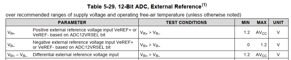
I am planning to use the Veref+ and Veref- ADC inputs In the data sheet, I cannot find a specification on the range of acceptable values of external ADC Channels or Verefs.
Is Veref+ capable of a value of DVCC? What if using the internal ADC Buffer?
Is Veref- capable of a value of DVSS?
If Veref- is set to a value between DVCC and DVSS, and the Channel Input is below the Veref-, can damage occur? Will the ADC result be zero or something unknown?
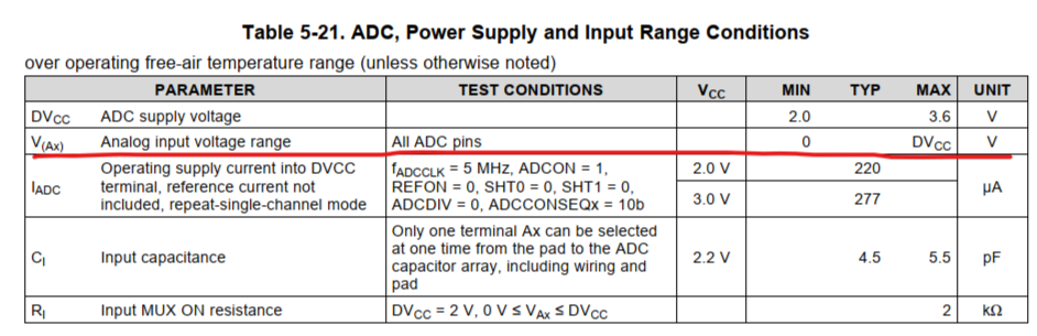
What is the input range spec for Channel inputs?
The multiplexed pin for Veref+ is also A0 and Veref- is also A2, according to the Datasheet (though there is discrepancy in Table 4-2, Signal Descriptions). When programming a sequence of conversions, the ADC always decrements to A0. If using Veref+ and Veref-, what will be the expected results of A0 and A2 conversions?