This thread has been locked.

If you have a related question, please click the "Ask a related question" button in the top right corner. The newly created question will be automatically linked to this question.

TM4C123GH6PM: Part Suitability and Confirmation on Flash size

Part Number: TM4C123GH6PM

I have a design which is based on STM32

but due to global IC shortage and few problems i dont want to go ahead with it,

so i am re designing the requirement again, as i am at a very early stage.

My architecture is simple i require 6 UART

4 UARTS are connected to RS422

2 UARTS are connected to RS232

in above one of the RS422 will behave as master sending data to other RS422 and RS232 ports and listens to other for incoming responses or messages

I have chosen  TM4C123GH6PM as my device as it has more than 6 UART and good clocking frequency and reference design of launch pad

below are my questions kindly answer

1. All the UARTS in  TM4C123GH6PM are functional at a time ? i mean are they independent and can work all at a time ? 

2. My code is simple, listening to UART 1 and multicasting data to other UARTs and reading responses from them, for which i would prefer bare metal code,

is 256kb of on chip flash sufficient ?

3. what is the End of Life of the part  TM4C123GH6PM

4. I can see the part being in good stock , will it be stocked even in the current global IC shortage ?

5. is there any pinmux tool for this IC ? or the only excel sheet ?

6. I have a XDS 200 debugger with me, will it be sufficient to flash the IC ?

7. can i configure each uart with different baud rate ?

  • Hi,

    1. All the UARTS in  TM4C123GH6PM are functional at a time ? i mean are they independent and can work all at a time ? 

    2. My code is simple, listening to UART 1 and multicasting data to other UARTs and reading responses from them, for which i would prefer bare metal code,

    is 256kb of on chip flash sufficient ?

    3. what is the End of Life of the part  TM4C123GH6PM

    4. I can see the part being in good stock , will it be stocked even in the current global IC shortage ?

    5. is there any pinmux tool for this IC ? or the only excel sheet ?

    6. I have a XDS 200 debugger with me, will it be sufficient to flash the IC ?

    7. can i configure each uart with different baud rate ?

    1. Yes.

    2. If your application is as simple as what you describe then I think 256kB will be sufficient. 

    3. There is no plan to EOF this product. In another word, you are looking at many many years of this product on the horizon. 

    4. I'm an engineer and I can't really speak for the global shortage. You might want to contact your local TI sales office for additional information. 

    5. Yes, please go to https://www.ti.com/tool/PINMUXTOOL or https://dev.ti.com/sysconfig/?fromPinmux=true#/start.

    6. XDS200 is good choice.

    7. Yes. 

  • Thanks for the response I have attached the Schematic i would like have your views on the same, kindly look in to TIVA and JTAG portion, i am also attaching pinmux tool file, in which i did not see any issues too, you may give a look.

    a. Schematic

    b. PINMUX

    apart from above attachment while doing schematic i had following doubts 

    1. Is it advised to tie the JTAG Reset to Actual Reset of Tiva ?

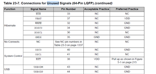
    2. I am not trying to put the Tiva in to Hibernation modes, so i have left it open, what to do with un-used ?

    3. I have followed the decoupling caps as used in the launch pad, hope they should be fine

    4. Confirm on the JTAG Header part, i am using xds200 probe, i have gone through multiple threads but could not find exact information of footprint numbering suggested for PCB Header and also i could not find exact pinout of xds200 wire header.

    5. Mainly i am skeptical on my JTAG wiring for connecting XDS200, kindly confirm it.

    6. last but very important doubt is maximum current consumption by VDD3V3 rail of MCU, from data sheet i can understand it to be 60mA, correct me if i am wrong, so 400mA regulator used on launch pad should be sufficient.

  • 1. Is it advised to tie the JTAG Reset to Actual Reset of Tiva ?

    2. I am not trying to put the Tiva in to Hibernation modes, so i have left it open, what to do with un-used ?

    3. I have followed the decoupling caps as used in the launch pad, hope they should be fine

    4. Confirm on the JTAG Header part, i am using xds200 probe, i have gone through multiple threads but could not find exact information of footprint numbering suggested for PCB Header and also i could not find exact pinout of xds200 wire header.

    5. Mainly i am skeptical on my JTAG wiring for connecting XDS200, kindly confirm it.

    6. last but very important doubt is maximum current consumption by VDD3V3 rail of MCU, from data sheet i can understand it to be 60mA, correct me if i am wrong, so 400mA regulator used on launch pad should be sufficient.

    1. That is up to you. I have seen people done that. 

    2. Which pins are your talking about? Please reference the unused pins section in the datasheet.

    3. it should be fine if you follow the LP schematic. Please also reference the TM4C123 system design guideline. https://www.ti.com/lit/pdf/spma059

    4. This app note should help. https://www.ti.com/lit/pdf/spma075

    5. Please see above app note in section 3.2 table 2. 

    6. Yes, 400mA regulator will be enough. Please also take into account other components on your board sourcing from the same regulator. 

  • 1. After seeing EVK schematics i am quite confused on nRST and TRST of cTI JTAG Interface, my intention is the Debugger must be able to reset the device when required, for which i asssume nRST is the signal pin num 15 to be used, is my assumption right ? what is the purpose of TRST then ?

    2.Current Consumption of my complete board is 60mA maximum for TIVA and 35mA for other devices like level converters, so i assume the existing 400mA LDO must do my need.

    3.I would request you to have a look at the attached schematic in previous reply and suggest for corrections, if there are any major blunders which would effect the functionality or boot up sequence.

  • Hi,

     Sorry for the late reply. Yesterday was a public holiday in the US. 

      The MCU does not have TRST input. The TRST is the reset pin for the TAP state machine. However, to reset the TAP state machine, you can also hold the TMS pin high for five cycles and can also force the TAP into idle state. In short, the TRST is for the JTAG, not a reset for the MCU core logic. 

      400mA should serve your need. 

      Looking at your schematic I see the CTI20 header. Although ok and I don't really see an issue, any reason you don't use ARM10 or ARM20 header. The ARM headers allow you to potentially use other debug probe that supports ARM processors. The XDS200 debug probe package should come with adapters from CTI-JTAG to ARM-JTAG.  

  • I fear that by mistake i may loose these small headers, which is why i am sticking to use the default header that can mate to probe directly.

    Currently i have only XDS200 In my lab