Part Number: EK-TM4C1294XL
Other Parts Discussed in Thread: ADS127L01, TM4C1294KCPDT, TM4C1294NCPDT
Tool/software: Code Composer Studio
Dear Sirs,
We want to send 32-bit data from the SPI output of an ADC board to the EK-TM4C1294XL.
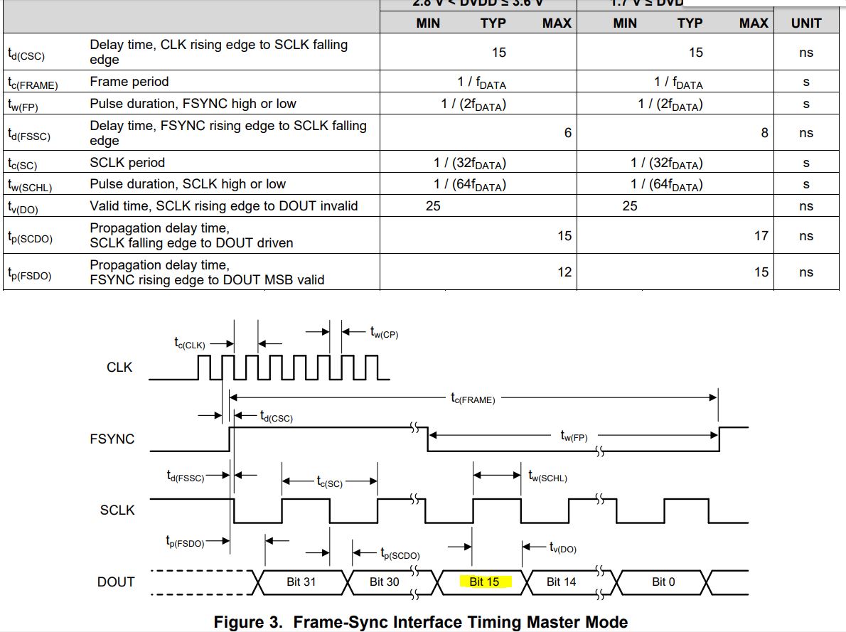
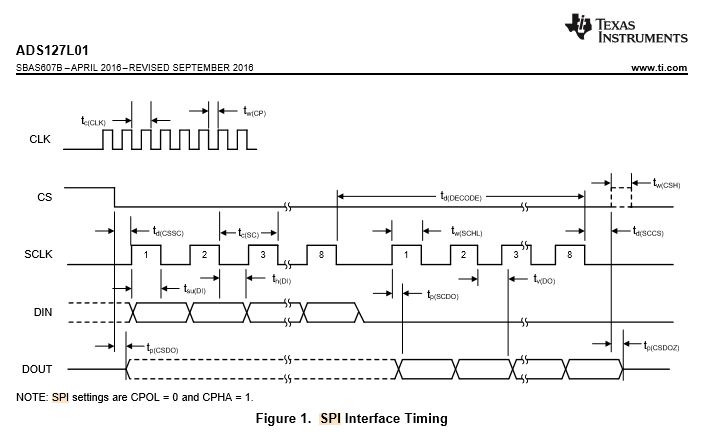
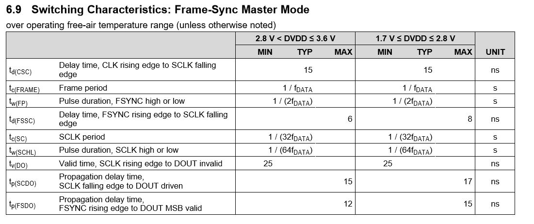
ADC Board is the SPI master: Texas Instruments EVM ADS127L01
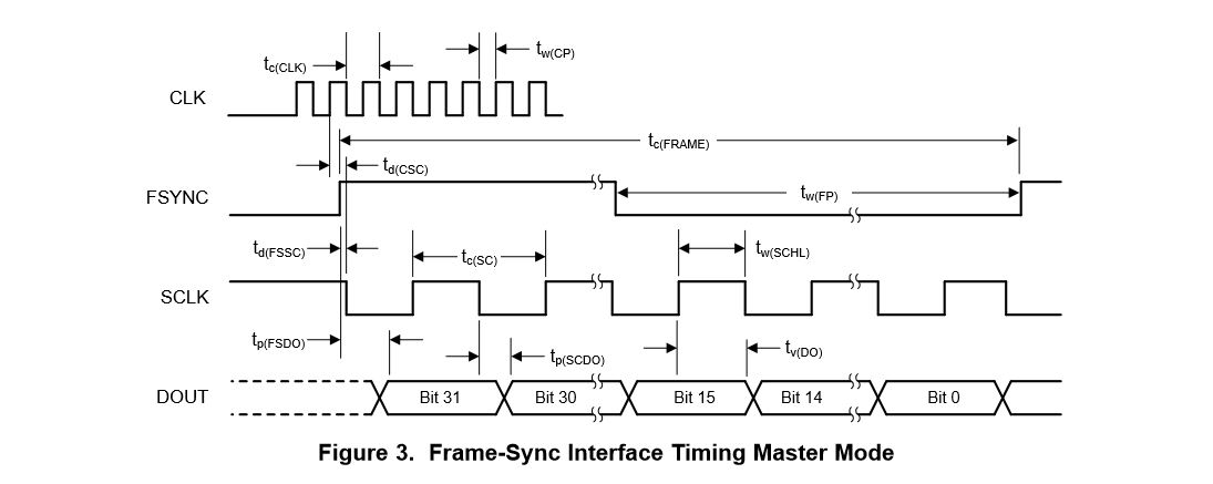
Selected Master SPI mode : Frame sync mode . EK-TM4C1294XL will be the slave. It will not send any data . It will only read.
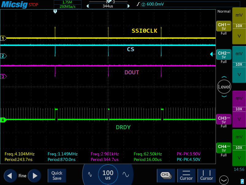
Used SPI outputs of the ADC board (master) : SCLK, FSYNC, DOUT .
We are not using CS (chip select) and DIN (data input), Because TM4C1294 will not send any data to the ADC board. It will only read data.
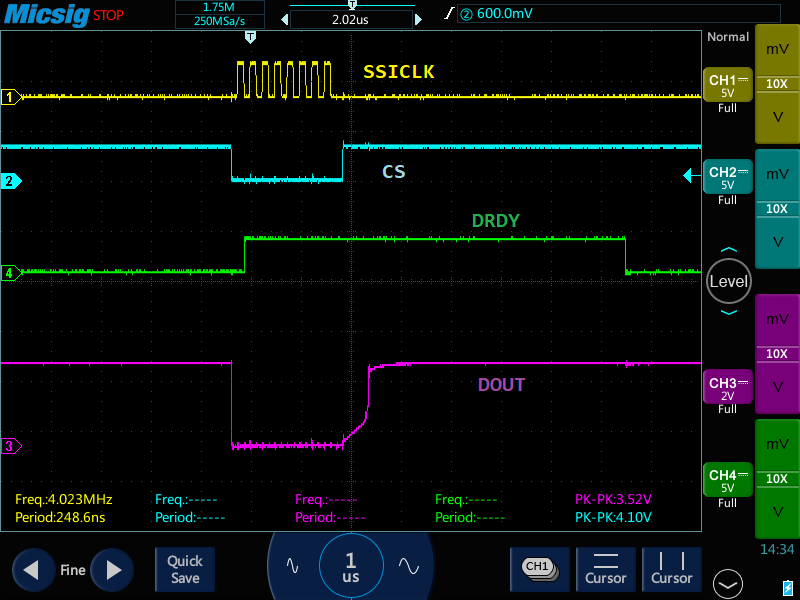
Interface timing is monitored and tested by oscilloscope. There are no problems.
32 bit (binary 2's complement data) can be seen on the DOUT terminal in each frame cycle synchronously. For testing the ADC board ,We have applied different voltage values
to the analogue input of ADC,then we wrote down the binary values from the screen of oscilloscope and decoded them manually. It was very good .
The data is at the door of the TM4C1294.
But we don't know how to put the 32 bit data into the TM4C1294. As we examined the data sheet of TM4C1294XL , what we have noticed, it has max of 16 bits wide input RX-FIFO register.
We are using an example SPI program. When we try to read the data, we saw inconsistent values on the CCS debugging console. We are sure that the frame synchronization does not happen properly.
As we understand ,our example SPI program has not suitable settings for our purpose.
May you recommend a method of reading that kind of data to the EK-TM4C1294XL ?
Best Regards,
Mete