This thread has been locked.

If you have a related question, please click the "Ask a related question" button in the top right corner. The newly created question will be automatically linked to this question.

CCS/EK-TM4C129EXL: Unable to read 32 bit values from ADC || Reading only 16-bit values

Part Number: EK-TM4C129EXL

Tool/software: Code Composer Studio

Experience Level: Beginner

With the help of responses from my previous forum post, I succeeded in establishing communication between ADC and  controller via SPI. 

Now, I'm able to read ID register. However, I'm not able to get data values properly.

Data sheet of the ADC - https://www.analog.com/media/en/technical-documentation/data-sheets/AD7177-2.pdf

Able to read ID register properly.

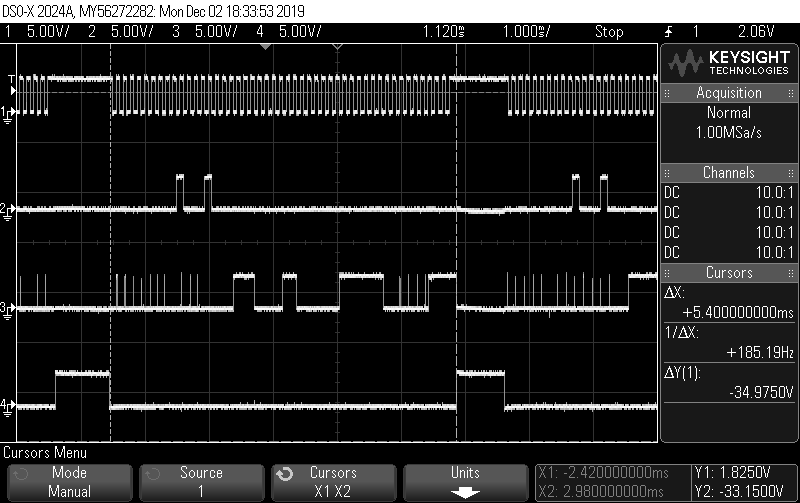
When trying to read Data Register, I get only 16-bit data instead of 32-bit data. I'm reading twice(by giving a read command for each 16-bit). I'm not sure if this is the right way, but if I give only 1 read command and try to read it twice, it is not able to read and is getting struck in the DataGet().

How do I read 32- bit data.

My algorithm is as follows:

1) Configure SPI communication in 16 bit, Mode-3

2) Configured GPIO interrupt for falling edges. Interrupt pin is connected to DOUT

 ISR is written in the following way:

1) Disable interrupt and clear flag(to make sure there's no successive interrupt while ISR() is being executed)

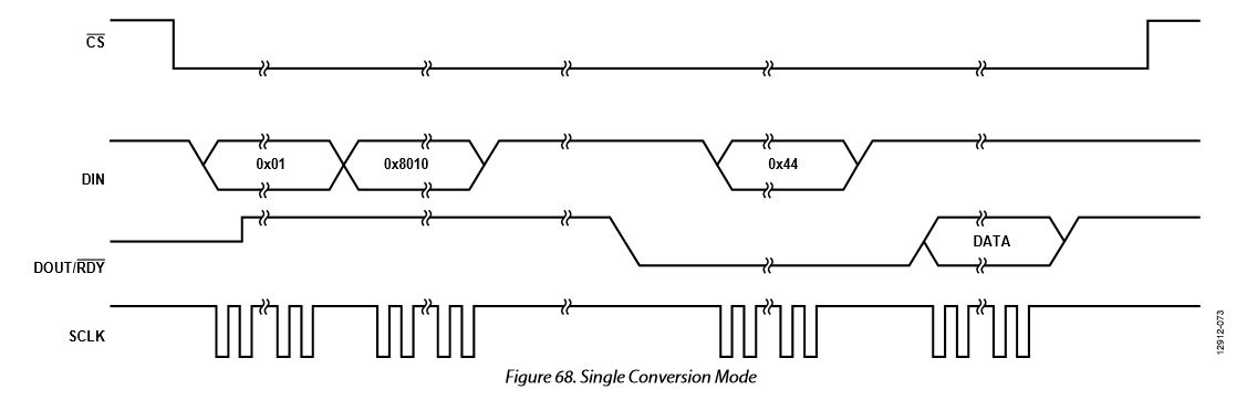
2) Read ID register (command word = 0x47)

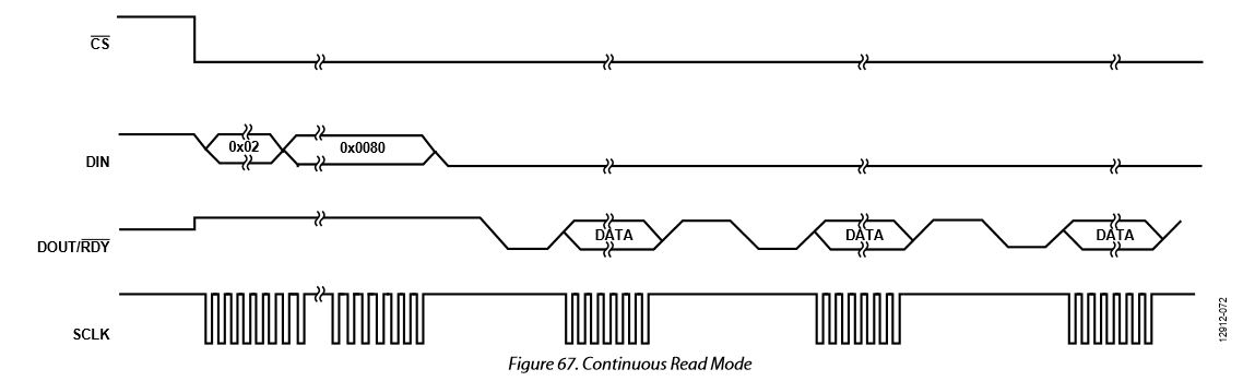
3) Write to IF mode register to make sure word length - 32 bits (command word = 0x02)

4) Write to data register to read it (comamand word = 0x44)

5) Read it (after 1st read, sending an other 0x44 command and then reading again) . Then, left shifting the MSB's by 16 and bitwise OR with LSB's 

6) Enable Interrupt

Results are as follows:

INPUT     - OUTPUT

-2.5 V      - around 0 (0)

-1.3 V     - around 16,000

0 V         - around 32,000(2^15)

1.3 V       - around  48,000

2.5 V      - around 64,000 (2^16)

As per the above readings, I'm inferring that I'm reading only 16-bit value and not 32- bit value.

I'm attaching my code to this post. Please help me get 32-bit values. Am I doing wrong in the configuration or the way I'm reading the values? or is there anything else that I'm missing out? Any leads would highly be appreciated. 

#include <stdbool.h>
#include <stdint.h>
#include "inc/hw_memmap.h"
#include "driverlib/gpio.h"
#include "driverlib/pin_map.h"
#include "driverlib/ssi.h"
#include "driverlib/sysctl.h"
#include "driverlib/uart.h"
#include "utils/uartstdio.h"
#include "inc/hw_types.h"
#include "inc/hw_ints.h"
#include "driverlib/adc.h"
#include "driverlib/interrupt.h"
#include "driverlib/rom.h"
#include "driverlib/rom_map.h"
#include "driverlib/fpu.h"
#include "driverlib/debug.h"

#include "drivers/pinout.h"


//*****************************************************************************
//
//! \addtogroup ssi_examples_list
//! <h1>SPI Master (spi_master)</h1>
//!
//! This example shows how to configure the SSI0 as SPI Master.  The code will
//! send three characters on the master Tx then polls the receive FIFO until
//! 3 characters are received on the master Rx.
//!
//! This example uses the following peripherals and I/O signals.  You must
//! review these and change as needed for your own board:
//! - SSI0 peripheral
//! - GPIO Port A peripheral (for SSI0 pins)
//! - SSI0Clk - PA2
//! - SSI0Fss - PA3
//! - SSI0Rx  - PA4
//! - SSI0Tx  - PA5
//!
//! The following UART signals are configured only for displaying console
//! messages for this example.  These are not required for operation of SSI0.
//! - UART0 peripheral
//! - GPIO Port A peripheral (for UART0 pins)
//! - UART0RX - PA0
//! - UART0TX - PA1
//!
//! This example uses the following interrupt handlers.  To use this example
//! in your own application you must add these interrupt handlers to your
//! vector table.
//! - None.
//
//*****************************************************************************

//*****************************************************************************
//
// Number of bytes to send and receive.
//
//*****************************************************************************
#define NUM_SSI_DATA     2
uint32_t g_ui32SysClock,flag=0;
uint32_t pui32DataRx[NUM_SSI_DATA];
uint32_t pui32DataRx_1[NUM_SSI_DATA];
uint32_t pui32DataTx_1[NUM_SSI_DATA];
    uint32_t ui32Index;
    uint32_t ID_REGISTER[2], temp;
//*****************************************************************************
//
// This function sets up UART0 to be used for a console to display information
// as the example is running.
//
//*****************************************************************************

void ISR();

void ConfigureUART(void)
{
    //
    // Enable the GPIO Peripheral used by the UART.
    //
    ROM_SysCtlPeripheralEnable(SYSCTL_PERIPH_GPIOA);

    //
    // Enable UART0
    //
    ROM_SysCtlPeripheralEnable(SYSCTL_PERIPH_UART0);

    //
    // Configure GPIO Pins for UART mode.
    //
    ROM_GPIOPinConfigure(GPIO_PA0_U0RX);
    ROM_GPIOPinConfigure(GPIO_PA1_U0TX);
    ROM_GPIOPinTypeUART(GPIO_PORTA_BASE, GPIO_PIN_0 | GPIO_PIN_1);

    //
    // Initialize the UART for console I/O.
    //
    UARTStdioConfig(0, 115200, g_ui32SysClock);
    //UARTprintf("UART configured successfully\n");
}


//*****************************************************************************
//
// Configure SSI0 in master Freescale (SPI) mode.  This example will send out
// 3 bytes of data, then wait for 3 bytes of data to come in.  This will all be
// done using the polling method.
//
//*****************************************************************************
void
main(void)
{

    /*
#if defined(TARGET_IS_TM4C129_RA0) ||                                         \
    defined(TARGET_IS_TM4C129_RA1) ||                                         \
    defined(TARGET_IS_TM4C129_RA2)
    uint32_t ui32SysClock;
#endif
*/

    g_ui32SysClock = MAP_SysCtlClockFreqSet((SYSCTL_XTAL_25MHZ |
            SYSCTL_OSC_MAIN | SYSCTL_USE_PLL |
            SYSCTL_CFG_VCO_480), 120000000);//Sets the clock Frequency
    ConfigureUART();
    //SysCtlPeripheralEnable(SYSCTL_PERIPH_GPIOA);
    SysCtlPeripheralEnable(SYSCTL_PERIPH_GPIOP);
    SysCtlPeripheralEnable(SYSCTL_PERIPH_SSI0);

   // PinoutSet(false, false);//enables the GPIO modules and configures the device pins for standard usages


    GPIOPinConfigure(GPIO_PA2_SSI0CLK);
    GPIOPinConfigure(GPIO_PA3_SSI0FSS);
    GPIOPinConfigure(GPIO_PA5_SSI0XDAT1);
    GPIOPinConfigure(GPIO_PA4_SSI0XDAT0);


    // The SSI0 peripheral must be enabled for use.
    //


    //
    // Configure the GPIO settings for the SSI pins.  This function also gives
    // control of these pins to the SSI hardware.  Consult the data sheet to
    // see which functions are allocated per pin.
    // The pins are assigned as follows:
    //      PA5 - SSI0Tx
    //      PA4 - SSI0Rx
    //      PA3 - SSI0Fss
    //      PA2 - SSI0CLK
    // TODO: change this to select the port/pin you are using.
    //
    GPIOPinTypeSSI(GPIO_PORTA_BASE, GPIO_PIN_5 | GPIO_PIN_4 | GPIO_PIN_3 |
                   GPIO_PIN_2);

    //
    // Configure and enable the SSI port for SPI master mode.  Use SSI0,
    // system clock supply, idle clock level low and active low clock in
    // freescale SPI mode, master mode, 1MHz SSI frequency, and 8-bit data.
    // For SPI mode, you can set the polarity of the SSI clock when the SSI
    // unit is idle.  You can also configure what clock edge you want to
    // capture data on.  Please reference the datasheet for more information on
    // the different SPI modes.
    //

//#if defined(TARGET_IS_TM4C129_RA0) ||                                         \
//    defined(TARGET_IS_TM4C129_RA1) ||                                         \
//    defined(TARGET_IS_TM4C129_RA2)
//    SSIConfigSetExpClk(SSI0_BASE, g_ui32SysClock, SSI_FRF_MOTO_MODE_3,
//                       SSI_MODE_MASTER, 300000, 16);
//#else
//    SSIConfigSetExpClk(SSI0_BASE, g_ui32SysClock, SSI_FRF_MOTO_MODE_3,
//                       SSI_MODE_MASTER, 300000, 16);
//#endif

    SSIConfigSetExpClk(SSI0_BASE, g_ui32SysClock, SSI_FRF_MOTO_MODE_3,
            SSI_MODE_MASTER, 300000, 16);

    //
    // Enable the SSI0 module.
    //
    //SSIAdvModeSet(SSI0_BASE, SSI_ADV_MODE_QUAD_WRITE);
   SSIAdvModeSet(SSI0_BASE, SSI_ADV_MODE_READ_WRITE);
   SSIEnable(SSI0_BASE);
    //SSIDataPut(SSI0_BASE,0x47);
   while(SSIDataGetNonBlocking(SSI0_BASE, &ID_REGISTER[0]))
        {
        }
    //SSIDataPut(SSI0_BASE,0x8274);
    //
    //ox29 -> Fliter Config 1
    //Filter - Sinc3 -> Bit word= 1000001001101000 = 0x8268
    //Filter - Sinc3 -> Bit word= 1000001001110100 =


//    while(SSIBusy(SSI0_BASE))
//        {
//        }
//    for(ui32Index = 0; ui32Index < 2; ui32Index++)
//            {
//
//                //
//                // Receive the data using the "blocking" Get function. This function
//                // will wait until there is data in the receive FIFO before returning.
//                //
//                SSIDataGet(SSI0_BASE, &pui32DataRx[ui32Index]);
//                //UARTprintf("Test print\n");
//                //
//                // Since we are using 8-bit data, mask off the MSB.
//                //
//                pui32DataRx[ui32Index] &= 0x000000FF;
//
//                //
//                // Display the data that SSI0 received.
//                //
//            //    UARTprintf("Received = ");
//            //    UARTprintf("'%d' ", pui32DataRx[ui32Index]);
//                while(SSIBusy(SSI0_BASE))
//                    {
//                    }
//
//            }

//        while(SSIBusy(SSI0_BASE))
//            {
//            }

    //
    // Read any residual data from the SSI port.  This makes sure the receive
    // FIFOs are empty, so we don't read any unwanted junk.  This is done hereT\n");


       SSIDataPut(SSI0_BASE,0x47);//Command word To read ID register
       SSIDataGet(SSI0_BASE,ID_REGISTER);
       SSIDataPut(SSI0_BASE,0x00);//Dummy data
       SSIDataGet(SSI0_BASE,&ID_REGISTER[0]);
       UARTprintf("ID: %d \n", ID_REGISTER[0]);


       SSIDataPut(SSI0_BASE,0x02); //IF Mode register command word
       SSIDataGet(SSI0_BASE,pui32DataRx);//Dummy read
   //    SysCtlDelay(g_ui32SysClock );//delay


       GPIOIntRegisterPin(GPIO_PORTP_BASE, GPIO_PIN_0, ISR);// Registering GPIO P0 as interrupt
       GPIOPinTypeGPIOInput(GPIO_PORTP_BASE, GPIO_PIN_0);
       GPIOIntTypeSet(GPIO_PORTP_BASE, GPIO_PIN_0, GPIO_FALLING_EDGE);
       GPIOIntEnable(GPIO_PORTP_BASE, GPIO_PIN_0);
       IntEnable(INT_GPIOP0);
        //UARTprintf("Test print\n");

             //IntTrigger(INT_GPIOP0);
        //UARTprintf("Interrupt configured successfully\n");


    //
    // Display indication that the SSI is transmitting data.
    //


    //UARTprintf("'%d' ", *temp);
    //UARTprintf("Sent:\n  ");
    //SSIDataGet(SSI0_BASE, &pui32DataRx[ui32Index]);

    //
    // Wait until SSI0 is done transferring all the data in the transmit FIFO.
    //


    //
    // Display indication that the SSI is receiving data.
    //
  //  UARTprintf("\nInterrupt not occurred\n  ");

    //
    // Receive 3 bytes of data.
    //
    //for(ui32Index = 0; ui32Index < NUM_SSI_DATA; ui32Index++)
  //  {
        //
        // Receive the data using the "blocking" Get function. This function
        // will wait until there is data in the receive FIFO before returning.
        //
        //SSIDataGet(SSI0_BASE, &pui32DataRx[0]);

        //
        // Since we are using 8-bit data, mask off the MSB.
        //
        //pui32DataRx[0] &= 0x0000FFFF;

        //
        // Display the data that SSI0 received.
        //
       // UARTprintf("'%d' ", pui32DataRx[ui32Index]);
//        while(SSIBusy(SSI0_BASE))
//            {
//            }
  //  }

    while(1)
    {
    }

    //
    // Return no errors
    //
    //return(0);*/

}

void ISR()
{
    //UARTprintf("Interrupt Occurred\n");
    GPIOIntClear(GPIO_PORTP_BASE,GPIO_PIN_0);
    GPIOIntDisable(GPIO_PORTP_BASE, GPIO_PIN_0);
    IntDisable(INT_GPIOP0);
//        SSIDataPut(SSI0_BASE,0x47);//Command word To read ID register
//           SSIDataGet(SSI0_BASE,ID_REGISTER);
//           SSIDataPut(SSI0_BASE,0x00);//Dummy data
//           SSIDataGet(SSI0_BASE,&ID_REGISTER[0]);
//           UARTprintf("ID: %d \n", ID_REGISTER[0]);


    //SSIDataGet(SSI0_BASE, &pui32DataRx[ui32Index]);

//    while(SSIDataGetNonBlocking(SSI0_BASE, &pui32DataRx_1[0]))
//       {
//       }

//        SSIDataPut(SSI0_BASE,0x00);
//        while(SSIBusy(SSI0_BASE))
//                            {
//                            }

    pui32DataRx_1[ui32Index] = 0x00000000;
//
//       SSIDataPut(SSI0_BASE,0x44);//Command word To read  register
//       SSIDataGet(SSI0_BASE,pui32DataRx_1); // dummy data
//       // Now read the two bytes of the ID
//       SSIDataPut(SSI0_BASE,0x00);//send dummy data
//       SSIDataGet(SSI0_BASE,&pui32DataRx_1[0]); // first byte
//
//    while(SSIBusy(SSI0_BASE))
//                    {
//                    }
//                while(SSIDataGetNonBlocking(SSI0_BASE, &pui32DataRx_1[ui32Index]))
//                        {
//                        }
//    SSIDataPut(SSI0_BASE,0x44);//Command word To read  register
//    SSIDataGet(SSI0_BASE,pui32DataRx); // dummy data
//
//    SSIDataPut(SSI0_BASE,0x00);//send dummy data
//    SSIDataGet(SSI0_BASE,&pui32DataRx[1]); // first byte
       //UARTprintf("ADC value: 0x%02x%02x\n", pui32DataRx[0], pui32DataRx[1]);

    for(ui32Index = 0; ui32Index < 2; ui32Index++)
        {

            //
            // Receive the data using the "blocking" Get function. This function
            // will wait until there is data in the receive FIFO before returning.

            SSIDataPut(SSI0_BASE,0x44);
            SSIDataGet(SSI0_BASE, pui32DataRx);//Reading dummy
            SSIDataPut(SSI0_BASE,0x00);//Writing dummy
            SSIDataGet(SSI0_BASE, &pui32DataRx[ui32Index]);//Reading the actual value
            //SSIDataGet(SSI0_BASE, &pui32DataRx[ui32Index]);
            //SSIDataPut(SSI0_BASE,0x00);
            //UARTprintf("Test print\n");
            //
            // Since we are using 8-bit data, mask off the MSB.
            //16-bit
            //pui32DataRx_1[ui32Index] &= 0x0000FFFF;

            //
            // Display the data that SSI0 received.
            //
            //UARTprintf("Received = ");
          //  UARTprintf("'%d' \n", pui32DataRx_1[ui32Index]);
            while(SSIBusy(SSI0_BASE))
                {
                }
            while(SSIDataGetNonBlocking(SSI0_BASE, &pui32DataRx[ui32Index]))
                    {
                    }
            //temp = pui32DataRx_1[0]<<16 | pui32DataRx_1[1] ;
            //pui32DataRx_1[ui32Index] &= 0x0000FFFF;

        }

   //temp = pui32DataRx[0] << 24 | pui32DataRx[1] << 16 | pui32DataRx[2] << 8 | pui32DataRx[3];
  temp = pui32DataRx[0]<<16 | pui32DataRx[1];


   UARTprintf("ADC value = '%d' \n", temp);
   //UARTprintf("ID: 0x%02x%02x\n", pui32DataRx[0], pui32DataRx[1]);
    GPIOIntEnable(GPIO_PORTP_BASE, GPIO_PIN_0);
    IntEnable(INT_GPIOP0);


}

  • Hi,

      Please read your respective datasheet again. This is an Analog device ADC. It says you need to give a 8-bit command. If this is the case, how can you configure the host MCU with 16-bit SPI length. Configure the MCU with 8-bit SPI size to give the command and read/write multiple of 8-bit data. 

  • Please also note that today is a major US holiday and response will be delayed. 

  • Greetings,

    May Staff & I (outsiders) well note the 'Excellence of your posting!'

    Your: 

    • description of objective
    • provision of detail
    • linking to the external device's data sheet  
    • sequential, numeric  listing    (believed clearer than that obtained from a 'narrative' ... you may note our group's allied, 'Use of Bullet Points!')
    • And - almost a first here, 'Experience Level.'

    Absolutely terrific.

    Now we (outsiders) are (nearly) at full staff today - and the quality of your post has, 'encouraged our response' - yet must await our 'Catching up w/our Order Book' and final tests & inspection of, 'Tech Goods which Ship tomorrow.'    We will try to respond today - yet kindly allow us a 'day's grace' - just in case.

    Do place high heed in vendor Charles' guidance - he has helped many.    It is hoped that a '2nd set of eyes' - even those of 'outsiders' - may further assist your 'solution.'

    [edit]:    Vendor's Charles has suspected that your post is a (slight) off-shoot from a 'highly similar' one.    Staff/I have already responded - in high detail - to that poster...

  • Dear Charles, 

    Thank you for your prompt response. I've made a note of your points and configured the SPI for 8 bit. In this case, I'm reading only 8-bit values i.e.,

    INPUT       -     OUTPUT

    -2.5 V        -      32,000 (2^15)

    0 V            -       8377516 (2^23)

    2.5V          -       16777216 (2^24)


    Please note that I've configured Word Length = 32 bit by writing to IF mode register(0x02).  I'm attaching my modified code here.

    Please correct me where I'm going wrong. Thank you for your time and patience

    #include <stdbool.h>
    #include <stdint.h>
    #include "inc/hw_memmap.h"
    #include "driverlib/gpio.h"
    #include "driverlib/pin_map.h"
    #include "driverlib/ssi.h"
    #include "driverlib/sysctl.h"
    #include "driverlib/uart.h"
    #include "utils/uartstdio.h"
    #include "inc/hw_types.h"
    #include "inc/hw_ints.h"
    #include "driverlib/adc.h"
    #include "driverlib/interrupt.h"
    #include "driverlib/rom.h"
    #include "driverlib/rom_map.h"
    #include "driverlib/fpu.h"
    #include "driverlib/debug.h"
    
    #include "drivers/pinout.h"


    //*****************************************************************************
    //
    //! \addtogroup ssi_examples_list
    //! <h1>SPI Master (spi_master)</h1>
    //!
    //! This example shows how to configure the SSI0 as SPI Master.  The code will
    //! send three characters on the master Tx then polls the receive FIFO until
    //! 3 characters are received on the master Rx.
    //!
    //! This example uses the following peripherals and I/O signals.  You must
    //! review these and change as needed for your own board:
    //! - SSI0 peripheral
    //! - GPIO Port A peripheral (for SSI0 pins)
    //! - SSI0Clk - PA2
    //! - SSI0Fss - PA3
    //! - SSI0Rx  - PA4
    //! - SSI0Tx  - PA5
    //!
    //! The following UART signals are configured only for displaying console
    //! messages for this example.  These are not required for operation of SSI0.
    //! - UART0 peripheral
    //! - GPIO Port A peripheral (for UART0 pins)
    //! - UART0RX - PA0
    //! - UART0TX - PA1
    //!
    //! This example uses the following interrupt handlers.  To use this example
    //! in your own application you must add these interrupt handlers to your
    //! vector table.
    //! - None.
    //
    //*****************************************************************************
    
    //*****************************************************************************
    //
    // Number of bytes to send and receive.
    //
    //*****************************************************************************
    #define NUM_SSI_DATA 4
    uint32_t g_ui32SysClock,flag=0;
    uint32_t pui32DataRx[NUM_SSI_DATA];
    
    uint32_t pui32DataRx_1[NUM_SSI_DATA];
    uint32_t pui32DataTx[NUM_SSI_DATA];
        uint32_t ui32Index;
        uint32_t ID_REGISTER[2], temp;
    //*****************************************************************************
    //
    // This function sets up UART0 to be used for a console to display information
    // as the example is running.
    //
    //*****************************************************************************
    
    void ISR();
    
    void ConfigureUART(void)
    {
        //
        // Enable the GPIO Peripheral used by the UART.
        //
        ROM_SysCtlPeripheralEnable(SYSCTL_PERIPH_GPIOA);
    
        //
        // Enable UART0
        //
        ROM_SysCtlPeripheralEnable(SYSCTL_PERIPH_UART0);
    
        //
        // Configure GPIO Pins for UART mode.
        //
        ROM_GPIOPinConfigure(GPIO_PA0_U0RX);
        ROM_GPIOPinConfigure(GPIO_PA1_U0TX);
        ROM_GPIOPinTypeUART(GPIO_PORTA_BASE, GPIO_PIN_0 | GPIO_PIN_1);
    
        //
        // Initialize the UART for console I/O.
        //
        UARTStdioConfig(0, 115200, g_ui32SysClock);
        //UARTprintf("UART configured successfully\n");
    }
    
    
    //*****************************************************************************
    //
    // Configure SSI0 in master Freescale (SPI) mode.  This example will send out
    // 3 bytes of data, then wait for 3 bytes of data to come in.  This will all be
    // done using the polling method.
    //
    //*****************************************************************************
    void
    main(void){
    
        /*
    #if defined(TARGET_IS_TM4C129_RA0) ||                                         \
        defined(TARGET_IS_TM4C129_RA1) ||                                         \
        defined(TARGET_IS_TM4C129_RA2)
        uint32_t ui32SysClock;
    #endif
    */
    
        g_ui32SysClock = MAP_SysCtlClockFreqSet((SYSCTL_XTAL_25MHZ |
                SYSCTL_OSC_MAIN | SYSCTL_USE_PLL |
                SYSCTL_CFG_VCO_480), 120000000);//Sets the clock Frequency
        ConfigureUART();
        //SysCtlPeripheralEnable(SYSCTL_PERIPH_GPIOA);
        SysCtlPeripheralEnable(SYSCTL_PERIPH_GPIOP);
        SysCtlPeripheralEnable(SYSCTL_PERIPH_SSI0);
    
       // PinoutSet(false, false);//enables the GPIO modules and configures the device pins for standard usages
    
    
        GPIOPinConfigure(GPIO_PA2_SSI0CLK);
        GPIOPinConfigure(GPIO_PA3_SSI0FSS);
        GPIOPinConfigure(GPIO_PA5_SSI0XDAT1);
        GPIOPinConfigure(GPIO_PA4_SSI0XDAT0);


        // The SSI0 peripheral must be enabled for use.
        //


        //
        // Configure the GPIO settings for the SSI pins.  This function also gives
        // control of these pins to the SSI hardware.  Consult the data sheet to
        // see which functions are allocated per pin.
        // The pins are assigned as follows:
        //      PA5 - SSI0Tx
        //      PA4 - SSI0Rx
        //      PA3 - SSI0Fss
        //      PA2 - SSI0CLK
        // TODO: change this to select the port/pin you are using.
        //
        GPIOPinTypeSSI(GPIO_PORTA_BASE, GPIO_PIN_5 | GPIO_PIN_4 | GPIO_PIN_3 |
                       GPIO_PIN_2);
    
        //
        // Configure and enable the SSI port for SPI master mode.  Use SSI0,
        // system clock supply, idle clock level low and active low clock in
        // freescale SPI mode, master mode, 1MHz SSI frequency, and 8-bit data.
        // For SPI mode, you can set the polarity of the SSI clock when the SSI
        // unit is idle.  You can also configure what clock edge you want to
        // capture data on.  Please reference the datasheet for more information on
        // the different SPI modes.
        //
    
    //#if defined(TARGET_IS_TM4C129_RA0) ||                                         \
    //    defined(TARGET_IS_TM4C129_RA1) ||                                         \
    //    defined(TARGET_IS_TM4C129_RA2)
    //    SSIConfigSetExpClk(SSI0_BASE, g_ui32SysClock, SSI_FRF_MOTO_MODE_3,
    //                       SSI_MODE_MASTER, 300000, 16);
    //#else
    //    SSIConfigSetExpClk(SSI0_BASE, g_ui32SysClock, SSI_FRF_MOTO_MODE_3,
    //                       SSI_MODE_MASTER, 300000, 16);
    //#endif
    
        SSIConfigSetExpClk(SSI0_BASE, g_ui32SysClock, SSI_FRF_MOTO_MODE_3,
                SSI_MODE_MASTER, 300000, 8);
    
        //
        // Enable the SSI0 module.
        //
        //SSIAdvModeSet(SSI0_BASE, SSI_ADV_MODE_QUAD_WRITE);
       SSIAdvModeSet(SSI0_BASE, SSI_ADV_MODE_READ_WRITE);
       SSIEnable(SSI0_BASE);
        //SSIDataPut(SSI0_BASE,0x47);
       while(SSIDataGetNonBlocking(SSI0_BASE, &ID_REGISTER[0]))
            {
            }


           GPIOIntRegisterPin(GPIO_PORTP_BASE, GPIO_PIN_0, ISR);// Registering GPIO P0 as interrupt
           GPIOPinTypeGPIOInput(GPIO_PORTP_BASE, GPIO_PIN_0);
           GPIOIntTypeSet(GPIO_PORTP_BASE, GPIO_PIN_0, GPIO_FALLING_EDGE);
           GPIOIntEnable(GPIO_PORTP_BASE, GPIO_PIN_0);
           IntEnable(INT_GPIOP0);


        while(1)
        {
        }
    
     
    }
    
    void ISR()
    {
        //UARTprintf("Interrupt Occurred\n");
        GPIOIntClear(GPIO_PORTP_BASE,GPIO_PIN_0);
        GPIOIntDisable(GPIO_PORTP_BASE, GPIO_PIN_0);
        IntDisable(INT_GPIOP0);
    
        SSIDataPut(SSI0_BASE,0x02); //IF Mode register command word
          SSIDataGet(SSI0_BASE,pui32DataRx);//Dummy read
    
    //        SSIDataPut(SSI0_BASE,0x47);//Command word To read ID register
    //           SSIDataGet(SSI0_BASE,ID_REGISTER);
    //           SSIDataPut(SSI0_BASE,0x00);//Dummy data
    //           SSIDataGet(SSI0_BASE,&ID_REGISTER[0]);
    //           UARTprintf("ID: %d \n", ID_REGISTER[0]);


    //    while(SSIDataGetNonBlocking(SSI0_BASE, &pui32DataRx_1[0]))
    //       {
    //       }
    
    //        SSIDataPut(SSI0_BASE,0x00);
    //        while(SSIBusy(SSI0_BASE))
    //                            {
    //                            }
    
     
                            }


        for(ui32Index = 0; ui32Index < NUM_SSI_DATA; ui32Index++)
            {
    
                //
                // Receive the data using the "blocking" Get function. This function
                // will wait until there is data in the receive FIFO before returning.
    
                SSIDataPut(SSI0_BASE,0x44);
                SSIDataGet(SSI0_BASE, pui32DataRx);//Reading dummy
                SSIDataPut(SSI0_BASE,0x00);//Writing dummy
                SSIDataGet(SSI0_BASE, &pui32DataRx[ui32Index]);//Reading the actual value
                
                //pui32DataRx_1[ui32Index] &= 0x0000FFFF;
    
                //
                // Display the data that SSI0 received.
                //
                //UARTprintf("Received = ");
              //  UARTprintf("'%d' \n", pui32DataRx_1[ui32Index]);
                while(SSIBusy(SSI0_BASE))
                    {
                    }
                while(SSIDataGetNonBlocking(SSI0_BASE, &pui32DataRx[ui32Index]))
                        {
                        }
                //temp = pui32DataRx_1[0]<<16 | pui32DataRx_1[1] ;
                //pui32DataRx_1[ui32Index] &= 0x0000FFFF;
    
            }
    
       temp = pui32DataRx[0] << 24 | pui32DataRx[1] << 16 | pui32DataRx[2] << 8 | pui32DataRx[3];
      //temp = pui32DataRx[0]<<16 | pui32DataRx[1];
    
    
       UARTprintf("ADC value = '%d' \n", temp);
       //UARTprintf("ID: 0x%02x%03x%04x%02x \n", pui32DataRx[0], pui32DataRx[1],pui32DataRx[2],pui32DataRx[3]);
       //UARTprintf("ID: 0x%02x%02x\n", pui32DataRx[0], pui32DataRx[1]);
       GPIOIntEnable(GPIO_PORTP_BASE, GPIO_PIN_0);
       IntEnable(INT_GPIOP0);


    }


  • Dear cb1_mobile,

    Thank you for your response. Could you please provide me the navigable link to that similar post? I tried to search but didn't succeed. Thank you for your time. Any other leads that you think will solve my issue would be highly appreciated. 

  • Thank you - 'young staff' - composers of our earlier, 'supportive response' - are 'pleased' to note your arrival.

    Past post (still highly (radio-active) : https://e2e.ti.com/support/microcontrollers/other/f/908/t/860078

    Note that the referenced post deals w/the sought, '32 bit, SPI Data Transfer.'    While differing (somewhat) from your (current) requirement - staff believes that 'key elements' w/in our postings (w/in that link) will, 'Inform & Advise' your efforts towards your objective.   (i.e. a 'General Method/Principle' was suggested - and as such - often best enables, 'Expansion & Adaptation/Accommodation of (even) differing objectives.')

  • Hi,

      I'm not familiar with the AD71772-2 device. However, reading its datasheet, it supports continuous conversion mode, continuous read mode and single conversion mode. Which mode are you intending to operate? Below is a timing diagram for single conversion mode. Can you please show a logic analyzer capture output to see if it matches the single conversion mode?

  • Dear Charles, 

    Firstly, Thank you for your response. I've configured it in Continuous Conversion Mode(which happens to be the default mode).
    Timing diagram available on pg: 37 of the data sheet. 

    I'm attaching the scope shots from my DSO.

    Image - 1 (CH-1 : DIN, CH-2 : DOUT)
    Image - 2 (CH-1 : DOUT, CH-2 : FSS)

    Please suggest me what do I do next. I had been struck here for quite a while now. The source code is in my previous reply on this post. How to read 32-bit value instead of 8/16 bit value.? (As of now I'm reading 8-bit when I'm configuring SPI in 8-bit mode and 16-bit when I'm configuring it in 16-bit mode) Any lead is highly appreciated. 

  • HI,

       Can you not capture your waveform with all four signals (CS, SCLK, DIN, DOUT/RDY) all probed on the same screen? It is really hard to see your signals in relation to each other, especially with the the presence of the SCLK. If you are operating in the continuous conversion mode then you need to reference the below diagram. Please note I'm not familiar with this third party's ADC. I'm reading its datasheet just like you.

      After you write the command (0x44) you should wait for the DOUT/RDY to go low. You can use an interrupt on falling edge of RDY. Once the processor is interrupted you can read the data. The datasheet shows that the CS remains active low. In your capture, I can't really make out what happened to the CS. It looks like it is going high every 8-bit word. Why don't you try to tie the CS low and see what happens? 


  • Greetings Charles,

    Charles Tsai said:
    Can you not capture your waveform with all four signals (CS, SCLK, DIN, DOUT/RDY) all probed on the same screen?

    Both your & my  'Weekend eyes & power of concentration' are surpassed by (young gurl) staff here - who (happily) note:

    "Is it not likely that poster has (only) a  2Ch Scope?"    Is it not (almost) time - for (some here) to, 'Get out of their way?'

  • On top of what I mentioned above, I have some more comments. 

      Why are you using advance mode? See below. Advance mode can only operate with SPO=0 and SPH=0. Your code configures for the SPI_MODE_3. Use the MODE_0 instead in legacy mode instead. 

    Your code configures the SPICLK at 300kHz. Isn't that too slow?Perhaps it is ok. I don't know how slow the ADC can go without affecting the current captured result. Is it possible that you are reading too slowly before the next conversion is complete and thus overwrites your current reading in the data register. Again, you need to find out this yourself. 

  • Dear Charles,

    Thank you for your timely response. I have done exactly the same thing which you said i.e., configured GPIO as interrupt and connected it to DOUT. To have a look at the code, please scroll up. 

    I'm attaching the screenshot of all 4 pins. As per Analog Devices, 32 clock pulses should be sent after 0x44 is written to DIN and I manually counted and there are eactly 32 pulses, which means as per the data sheet it has to give a 32 bit value.

    A small update in the past 3 days is that:

    1) There are a lot of unwanted interrupts triggering i.e., interrupt is occurring more than expected no. of times even when DOUT is not going low && CS = HIGH
    2) I ran a code by just configuring SSI and GPIO Interrupt with only a test print line in ISR(). I tried by tying the CS to both logic 0 and logic 1. Even when CS was high, interrupt was occurring. Please note that as per data sheet, DOUT will go low only after word is ready && CS=LOW. But in my case it is occurring due to the falling edge of some pulse 
    3) I'm assuming that few interrupts are occurring due to noise. (On scope I saw a random sine wave with 700 mV peak-peak in this case).
    4) From this, I'm inferring that one of the biggest glitches here could be false interrupts
    Please correct me if I'm wrong. If I'm right, how do I eliminate these interrupts due to noise? Is there any software solution to cancel this noise or increase the falling edge threshold.

    If you'v any other leads that could potentially solve my issue, I shall be more than glad to take your inputs. Struck here for a long time now, please help!

  • Hi,

      As much as I'd like to help you, but my expertise is limited to the MCU only. I would strongly recommend you check with Analog Device as to why the DOUT is glitches as shown in your capture. They are the experts of their products and should be able to help you troubleshoot their products much better than I can. The glitches on the DOUT line even when the CS is inactive can still mis-trigger a interrupt. With that said, I do have some comments.

    1. I thought you were going to change to a 8-bit command. However, from you capture, you are giving three 16-bit back-to-back commands. Are you sure you can give 16-bit command? Please consult with your ADC device vendor. Show them your capture and they should be able to comment if 16-bit command is valid. From my interpretation of their datasheet, you need to give an 8-bit command. 

    2. From the capture, there are a few glitches on the DOUT line even before the the 0x44 is sent on the DIN. Why are these glitches? I'm just as curious as you are. You ADC vendor can help on this question.

    3. I see in your ISR, you call the UARTprintf(). I think you should comment it out during your experiment. Calling UARTprintf() in an ISR is never good. The UARTprintf() can take many cycles to complete because the UART baudrate is much slower than the SSI ISR. You can miss an intended interrupt which are to occur in the future if you stay in the ISR too long. The ISR normally should be kept as short and quick as possible. When you are in the ISR, you can set a global flag and then exit the ISR. In your main() you can wait for the flag to set and then process the data. If you don't want to do it this way, you should at least comment out the UARTprintf() first. 

    4.  Perhaps you have updated your code. In your original pasted code, you only have two SSIDataPut(). If you are going to read three 8-bit data then you need to have a total of 4 SSIDataPut() in your ISR, isn't? The first one would be to write command 0x44 and another three dummy writes to provide SCLK to the ADC device to read the data. 

    5. Why don't you start with just 'one' single conversion instead of continuous conversion. If you can get just one conversion to work, I think it will be easier to expand onto other operating modes. 

    Why don't you contact your ADC vendor and ask them to provide an example waveform capture on how to read the data. Show how many clocks are need to read the Data Register properly in your desired mode. 

  • Dear Charles,

    Thank you for your reply. Here are the updates and methods I've tried:

    I have changed it again to 8-bit mode as per your suggestion. I'm attaching the latest scope shot here. The reason I've choose 'Continuous Conversion Mode' over other modes is because this is the default mode of ADC. I tried changing it to 'Continuous Read' and 'Single Conversion' modes but I didn't succeed. I tried writing to one of the RW registers(both IFMODE and ADCMODE) and reading back the same registers but I didn't succeed in that either. Due to all those failures, I'm sticking to read the 32-bit word from the data register. Since I need to get 32-bit values in CC mode ASAP for the project + it is the default mode+ failures in reading back registers and changing mode, I had no choice but to stick to default config(CC mode)).

    The code and scope shot I'm attaching now are the latest ones I'm using. Two important concerns I've at the MCU end are:

    1) False interrupts i.e., interrupts due to noise fluctuations ( How do I eliminate them?)
    2) Am I making any mistakes in reading the values or bit manipulation or SSI configuration ?

    I'm in touch in Analog Devices(AD) as well. Their suggestion(for 8-bit SPI master) was "You need to apply exactly 32 clock pulses after DIN in order to read a 32 bit value). On the scope, it looks like exactly 32 CLK pulses are being applied. The SCLK frequency should be in the range 319.601kHz to 20MHz as per AD. They advised me to do only the reading part in ISR(). However I am not able to do that because of false interrupts i.e., due to noise, ISR() is being executed continuously and if I don't have 0x44 in ISR() I only read 0's. Therefore, I'm forced to use 0x44 in ISR(). 

    Note:

    1) 0x02 in main() is only to ensure that Word Length = 32 bits
    2) I tried putting the 0x44 in while(1) and only reading part in ISR() but I read only 0's in this case
    3) I tried to comment out 0x02 and put only 0x44 in while(1), still no success

    #include <stdbool.h>
    #include <stdint.h>
    #include "inc/hw_memmap.h"
    #include "driverlib/gpio.h"
    #include "driverlib/pin_map.h"
    #include "driverlib/ssi.h"
    #include "driverlib/sysctl.h"
    #include "driverlib/uart.h"
    #include "utils/uartstdio.h"
    #include "inc/hw_types.h"
    #include "inc/hw_ints.h"
    #include "driverlib/adc.h"
    #include "driverlib/interrupt.h"
    #include "driverlib/rom.h"
    #include "driverlib/rom_map.h"
    #include "driverlib/fpu.h"
    #include "driverlib/debug.h"
    
    #include "drivers/pinout.h"
    
    
    #define NUM_SSI_DATA  4
    uint32_t g_ui32SysClock,flag=0, a = 0;
    uint32_t pui32DataRx[NUM_SSI_DATA];
    uint32_t pui32DataTx[NUM_SSI_DATA];
    uint32_t ui32Index;
    uint32_t ID_REGISTER[2], temp;
    
    
    void ISR();
    
    void ConfigureUART(void)
    {
        ROM_SysCtlPeripheralEnable(SYSCTL_PERIPH_GPIOA);
        ROM_SysCtlPeripheralEnable(SYSCTL_PERIPH_UART0);
        ROM_GPIOPinConfigure(GPIO_PA0_U0RX);
        ROM_GPIOPinConfigure(GPIO_PA1_U0TX);
        ROM_GPIOPinTypeUART(GPIO_PORTA_BASE, GPIO_PIN_0 | GPIO_PIN_1);
        UARTStdioConfig(0, 115200, g_ui32SysClock);
    }
    
    void main(void){
        g_ui32SysClock = MAP_SysCtlClockFreqSet((SYSCTL_XTAL_25MHZ |
                SYSCTL_OSC_MAIN | SYSCTL_USE_PLL |
                SYSCTL_CFG_VCO_480), 120000000);//Sets the clock Frequency
        ConfigureUART();
    
        SysCtlPeripheralEnable(SYSCTL_PERIPH_GPIOP);
        SysCtlPeripheralEnable(SYSCTL_PERIPH_SSI2);
        SysCtlPeripheralEnable(SYSCTL_PERIPH_GPIOD);
        
        GPIOPinConfigure(GPIO_PD3_SSI2CLK);
        GPIOPinConfigure(GPIO_PD2_SSI2FSS);
        GPIOPinConfigure(GPIO_PD0_SSI2XDAT1);
        GPIOPinConfigure(GPIO_PD1_SSI2XDAT0);
       
        GPIOPinTypeSSI(GPIO_PORTD_BASE, GPIO_PIN_1 | GPIO_PIN_0 | GPIO_PIN_3 |
                               GPIO_PIN_2);
    
        SSIConfigSetExpClk(SSI2_BASE, g_ui32SysClock, SSI_FRF_MOTO_MODE_3,
                SSI_MODE_MASTER, 2000000, 8);
    
     
        SSIAdvModeSet(SSI2_BASE, SSI_ADV_MODE_READ_WRITE);
        SSIEnable(SSI2_BASE);
      
    
        SSIDataPut(SSI2_BASE,0x02); //IF Mode register command word
        SSIDataGet(SSI2_BASE,pui32DataRx);//Dummy read
    
        GPIOIntRegisterPin(GPIO_PORTP_BASE, GPIO_PIN_1, ISR);// Registering GPIO P1 as interrupt
        GPIOPinTypeGPIOInput(GPIO_PORTP_BASE, GPIO_PIN_1);
        GPIOIntTypeSet(GPIO_PORTP_BASE, GPIO_PIN_1, GPIO_FALLING_EDGE);
        GPIOIntEnable(GPIO_PORTP_BASE, GPIO_PIN_1);
        IntEnable(INT_GPIOP1);


        while(1)
        {
            SSIDataPut(SSI2_BASE,0x44);
            SSIDataGet(SSI2_BASE,pui32DataRx);
    
        }
    
      
    }
    
    void ISR()
    {
    
        GPIOIntClear(GPIO_PORTP_BASE,GPIO_PIN_1);
        GPIOIntDisable(GPIO_PORTP_BASE, GPIO_PIN_1);
        IntDisable(INT_GPIOP1);
    
    
        SSIDataPut(SSI2_BASE, 0x44);
        SSIDataGet(SSI2_BASE, pui32DataRx);//Reading dummy
    
        SSIDataPut(SSI2_BASE,0x00);//Writing dummy
        SSIDataGet(SSI2_BASE, &pui32DataRx[0]);//Reading the actual value
    
        SSIDataPut(SSI2_BASE,0x00);//Writing dummy
        SSIDataGet(SSI2_BASE, &pui32DataRx[1]);//Reading the actual value
    
        SSIDataPut(SSI2_BASE,0x00);//Writing dummy
        SSIDataGet(SSI2_BASE, &pui32DataRx[2]);//Reading the actual value
                              
        SSIDataPut(SSI2_BASE,0x00);//Writing dummy
        SSIDataGet(SSI2_BASE, &pui32DataRx[3]);//Reading the actual value


       temp = pui32DataRx[0] << 24 | pui32DataRx[1] << 16 | pui32DataRx[2] << 8 | pui32DataRx[3];
    
    
      // UARTprintf("ADC value = '%d' \n", temp);
      
       GPIOPinWrite(GPIO_PORTA_BASE, GPIO_PIN_2, GPIO_PIN_2);
       GPIOIntEnable(GPIO_PORTP_BASE, GPIO_PIN_1);
       IntEnable(INT_GPIOP1);


    }

    Screenshot : CS, DIN, DOUT, SCLK with i/p voltage = 0V. Vref = 2.5V

    Observations are as follows:

    Input Voltage = 2.5V , Output = 2^24
    Input voltage = 0V ,  Output = 8424045 (2^23)
    Input Voltage = -2.5 ,   Output = 32,000 (2^15)

    All other configurations used are default configurations.

  • Hello again,

    Charles is by far the expert in regards to this MCU.     My 'outsider' group (may) be able to assist w/your Noise and/or Implementation Issues.

    Pranav Deep said:
    1) False interrupts i.e., interrupts due to noise fluctuations ( How do I eliminate them?)

    We have successfully resolved 'hundreds' of such noise issues - these points may prove helpful:

    • What is your 'basis' for attributing the 'false interrupts' to 'noise fluctuations?'    (i.e. What Noise - sourced by what? - located where? how detected & measured?)   Pardon but 'noise fluctuations' is so broad it proves, 'Not compelling (helpful).'
    • Is this ADI device mounted upon an ADI Eval/Development board?     Devices of this (potential) quality 'NEVER' perform well - when mounted upon breadboards.
    • Have you double/triple checked the existence of a proper, 'Common Ground' - between the (hoped for) ADC board & your MCU board?
    • Are both the MCU board and ADC board - powered from the same power source?    Have you 'scoped' the ADC's power pins - while 'in operation?'
    • How have you 'interconnected' between both boards?   (ADC & MCU boards)    If simply 'wired together' you may consider
      • employing shielded cable for the interconnect
      • shortening the cable/wire length - as much as possible
      • optically coupling between (each channel) but especially upon the SPI Clock line
    • What is the separation distance between these boards?    Can that distance be shortened?
    • Is the ADC board being properly (sufficiently) powered?   ('stealing' power from the MCU board - while convenient - may introduce noise & may prove insufficient.     Have you scoped the power pin(s) - at the ADC - while 'In opeation?'
    • Have you inserted a small 'RC network' - as close as possible to the MCU's 'interrupt pin' - in the attempt to suppress those 'glitch/false' signals?     There should be a 'compromise value' - sufficient to reduce and/or eliminate the glitch (as felt at the MCU) - yet not impacting the 'desired/real' ADC output signal.
    • As an experiment - can you 'excite the ADC via a 'quality Signal Generator' - at the lowest ADC spec'ed rate - observing for those 'false interrupts emitted by DRdy?    Short & direct connections (especialy between Generator & ADC board's Ground - are a MUST.
    • You should disable any/all 'Noise Sources' or high frequency operations - which may be causing your issue.    Relays, Switching Power Supplies, and any Power Components (especially when switching) ALL are suspect.
    • And - not what you 'wish to hear' - might ANY form of, 'Errant/Excessive Signal' been applied to this ADC?   (even briefly)    Were proper (written) ESD Safeguards in place & enforced - at all times - during the handling & installation of this ADC?    We've noted that 'Handling' is often lax (relaxed) during the excitement of, 'Working w/an advanced new device and/or board' - such proves NOT a 'rare issue!'

    Beyond these 'Noise Identification & Resolution Tactics' - it is always recommended to, 'Simplify & Restrict the MCU's Operation - when attempting to 'Manage such issues.'    Ideally - your MCU will execute, 'ONLY that code which directly addresses the ADC!'    It is especially important to, 'Disable all 'Non-SPI Interrupts' - and enable the code to access the ADC at dedicated intervals.   (perhaps triggered by the press of an MCU, board-mounted push-button.)

    Your opening posting - as earlier noted - was deemed 'superb.'   (Good that)    However your scope caps do NOT label the various channels - placing added 'search & time effort' upon your helpers.    (that's not to your advantage - the scope may enable such labeling - if not - you may import the scope cap into 'Paint' or similar - and add the labels.)   Minus those labels - in time - even 'you' may become confused!

    While the ADC IS expensive - so too the time/energy expended by, 'You & your remote helpers.'    Always it is (beyond) useful to acquire multiple identical devices (boards in this case) - and to carefully examine if 'Issues persist identically - from board to board.'    Single Device (or board) 'anomalies' do exist - and consume thousands of 'Skilled Man-Hours' - too often - chasing 'ghosts.'

  • This posting aims towards, 'Informing/Advising' a better means to (effectively) include Scope Caps.

    Note that this thread employs a highly complex, external IC (an ADC) - and even after 'multiple reads' - by both vendor agent & my outsider group - uncertainty still exists.    Scope caps should NOT 'Add to the complexity!'

    It is always useful to, 'Overlap the Scope Cap' w/the device's timing chart.   (at least to present each - as similarly  as possible.)   That said:

    The ADC's timing chart (Single Conversion):

    and now (Continuous Conversion)

    Note the duplication (in signal placement) between the modes.

    And then poster's scope cap -  strangely, 'Deviates from that signal placement - while being 'unlabeled.'   Yet earlier - this poster was 'praised' for the clear thought & effort - revealed w/in his opening post!

    Anything which reduces 'diagnostic ease' while 'adding time & effort' - proves NOT to (any/all) posters' (multiple posters) benefit.    A clear poster goal should be to 'help' the (would be) helpers...

  • While continuing to, 'Feel your & vendor Charles' pain' - may a (reasonable) solution be (already) at hand?     My crack staff & I have reviewed all '16 back-forth posts' - and must conclude that your very first posting - most likely - 'Effectively Succeeded - thus, Should have satisfied!'

    Note too - that initial, 16-bit harvesting of ADC data - apparently 'escaped' the horror of 'phantom interrupts' and vague noise complications.

    Let's review - that 1st post reported:

    Results are as follows:

    INPUT - OUTPUT

    -2.5 V - around 0 (0)
    -1.3 V - around 16,000
    0 V - around 32,000(2^15)
    1.3 V - around 48,000
    2.5 V - around 64,000 (2^16)

    You then wrote, "As per the above readings, I'm inferring that I'm reading only 16-bit value and not 32- bit value."

    These results - while indicative of '16 bits' - do indeed present the expected ADC's ranging performance.    (i.e. 0V - the ADC's bipolar 'mid-point' reports a voltage (exactly) centered between -2V5 (-2.5V old world) and +2V5.     Note that after you, 'Departed from this code' - all subsequent ADC measures produced 'grossly inaccurate measures!'

    Now you noted 'Only 16-bit values' - yet those were the 'most significant' such values - thus 'Highly Usable!'    (Your ADC presents MSb first.)    

    Why do you - as an (admitted) 'Beginner' (yet a resourceful & skilled one) seek beyond 16 bits?    It is rare that 'beyond 16 bits is required' - and most often - extremely difficult to achieve (both) accurate & precise results - at (even) 20 bits!     (my present firm - and several earlier - have earned (significant) 'Sales Income' - and only rarely have provided 20 bit ADC capability!    (a clear struggle)     Note too - those (pardon) 'Excess bits' will exact a rather severe, Conversion Delay upon your ADC measurements.    (i.e. your ADC notes a maximum scan rate of 10kSPS - yet this vendor's MCU converts 100 times faster!     And - (only) 19 of your ADC's bits are reported as 'Noise Free' - which means, 'ALL 16 of your most significant bits' are of great accuarcy!)   

    Thus your '16 bit results' should prove 'highly acceptable' - as this background info/analysis - strives to convey.     Don't you agree?

    If you make the effort to present properly 'labeled' scope traces (as detailed) & any modifications to your (opening post's code - which correctly 'harvested 16 bit ADC results' - my group (may) be able to devise an inventive means by which you (may), 'increase the number of ADC bits received.'    Although it remains 'doubtful' that such 'extra resolution' is (really) needed.    (most hi-resolution ADCs serve, 'Unusually high Dynamic signal ranging' - far from the 'norm' for those 'new to the subject...')

  • Dear cb1_mobile,

    Thank you for your response. The machine that we are developing is a high precision device and the data acquisition is very critical in our case. So it is mandatory that I get 32 bit values from this ADC.

    I've noted your points w.r.to labeling the scope shots and I shall label them properly before uploading anything from here on. As of now, I'm looking for debugging method/solutions w.r.to how I get 32 bit values from this ADC. Please note that my 1st code of this post(thought gave reliable 16-bit o/p) was configured as 16 bit SPI master. Upon Charles'(and Analog Devices') advice, I've modified to 8-bit mode. And also, given the time frame I'm dealing with it is essential that I get reliable 32-bit o/p from Continuous Conversion Mode ASAP, which also happens to be the default mode. I've already mentioned I didn't succeed when I tried to change to Continuous Read or Single Conversion mode and hence eliminated those options for now.

    With respect to false/unwanted interrupts. I cannot guarantee that it is because of noise or I don't have any idea about the source of noise. As you rightly mentioned noise is a vague description but I didn't have any better word to mean "random interrupts". I'm using a custom soldered board on which ADC is mounted. Connections are made with generic jumpers. They don't seem lose/tangled. I tried using a pull up, connecting an RC network(different combinations), decoupling capacitor, using a pull up resistor etc but didn't really succeed. Powering the MCU via USB. So, if this is an issue, then I'll have to make quite a few changes. Please note that no other devices are connected to the MCU except these pins.  Using bread board only to make a ground connection. All other connections are made using jumpers. I've tried almost all other methods you've suggested except exciting the ADC with a signal generator. The reason I didn't do that is, interrupt is occurring even when the jumper is not connected to DOUT(i.e., when is in air). Tried grounding the interrupt pin, then it is stable). 

    To sum up the 2 major issues:

    1) False interrupts
    2) Reading values ranging from 2^15 to 2^24 (Need to read 32 bit values)

    Once again, I'm attaching the labelled scope shot and the code in this reply. Please suggest me what I can do.

    #include <stdbool.h>
    #include <stdint.h>
    #include "inc/hw_memmap.h"
    #include "driverlib/gpio.h"
    #include "driverlib/pin_map.h"
    #include "driverlib/ssi.h"
    #include "driverlib/sysctl.h"
    #include "driverlib/uart.h"
    #include "utils/uartstdio.h"
    #include "inc/hw_types.h"
    #include "inc/hw_ints.h"
    #include "driverlib/adc.h"
    #include "driverlib/interrupt.h"
    #include "driverlib/rom.h"
    #include "driverlib/rom_map.h"
    #include "driverlib/fpu.h"
    #include "driverlib/debug.h"
    
    #include "drivers/pinout.h"
    
    
    #define NUM_SSI_DATA  4
    uint32_t g_ui32SysClock,flag=0, a = 0;
    uint32_t pui32DataRx[NUM_SSI_DATA];
    
    
    uint32_t pui32DataTx[NUM_SSI_DATA];
        uint32_t ui32Index;
        uint32_t ID_REGISTER[2], temp;
    
    void ISR();
    
    void ConfigureUART(void)
    {
       
        ROM_SysCtlPeripheralEnable(SYSCTL_PERIPH_GPIOA);
    
        ROM_SysCtlPeripheralEnable(SYSCTL_PERIPH_UART0);
    
        ROM_GPIOPinConfigure(GPIO_PA0_U0RX);
        ROM_GPIOPinConfigure(GPIO_PA1_U0TX);
        ROM_GPIOPinTypeUART(GPIO_PORTA_BASE, GPIO_PIN_0 | GPIO_PIN_1);
    
        
        UARTStdioConfig(0, 115200, g_ui32SysClock);
    
    }
    
    
    void main(void){
    
    
        g_ui32SysClock = MAP_SysCtlClockFreqSet((SYSCTL_XTAL_25MHZ |
                SYSCTL_OSC_MAIN | SYSCTL_USE_PLL |
                SYSCTL_CFG_VCO_480), 90000000);//Sets the clock Frequency
        ConfigureUART();
        
        SysCtlPeripheralEnable(SYSCTL_PERIPH_GPIOP);
        SysCtlPeripheralEnable(SYSCTL_PERIPH_SSI2);
        SysCtlPeripheralEnable(SYSCTL_PERIPH_GPIOD);


          GPIOPinConfigure(GPIO_PD3_SSI2CLK);
          GPIOPinConfigure(GPIO_PD2_SSI2FSS);
          GPIOPinConfigure(GPIO_PD0_SSI2XDAT1);
          GPIOPinConfigure(GPIO_PD1_SSI2XDAT0);
    
          GPIOPinTypeSSI(GPIO_PORTD_BASE, GPIO_PIN_1 | GPIO_PIN_0 | GPIO_PIN_3 |
                               GPIO_PIN_2);
    
     
          SSIConfigSetExpClk(SSI2_BASE, g_ui32SysClock, SSI_FRF_MOTO_MODE_3,
                SSI_MODE_MASTER, 10000000, 8);
    
       
       SSIAdvModeSet(SSI2_BASE, SSI_ADV_MODE_READ_WRITE);
       SSIEnable(SSI2_BASE);


           SSIDataPut(SSI2_BASE,0x02); //IF Mode register command word
           SSIDataGet(SSI2_BASE,pui32DataRx);//Dummy read


            GPIOIntRegisterPin(GPIO_PORTP_BASE, GPIO_PIN_1, ISR);// Registering GPIO P1 as interrupt
            GPIOPinTypeGPIOInput(GPIO_PORTP_BASE, GPIO_PIN_1);
            GPIOIntTypeSet(GPIO_PORTP_BASE, GPIO_PIN_1, GPIO_FALLING_EDGE);
            GPIOIntEnable(GPIO_PORTP_BASE, GPIO_PIN_1);
            IntEnable(INT_GPIOP1);
    
        while(1)
        {
            SSIDataPut(SSI2_BASE,0x44);
            SSIDataGet(SSI2_BASE,pui32DataRx);
    
        }
    
    }
    
    void ISR()
    {
    
        GPIOIntClear(GPIO_PORTP_BASE,GPIO_PIN_1);
        GPIOIntDisable(GPIO_PORTP_BASE, GPIO_PIN_1);
        IntDisable(INT_GPIOP1);
    
    
        SSIDataPut(SSI2_BASE, 0x44);
        SSIDataGet(SSI2_BASE, pui32DataRx);//Reading dummy
    
        SSIDataPut(SSI2_BASE,0x00);//Writing dummy
        SSIDataGet(SSI2_BASE, &pui32DataRx[0]);//Reading the actual value
                            
    
        SSIDataPut(SSI2_BASE,0x00);//Writing dummy
        SSIDataGet(SSI2_BASE, &pui32DataRx[1]);//Reading the actual value
    
        SSIDataPut(SSI2_BASE,0x00);//Writing dummy
        SSIDataGet(SSI2_BASE, &pui32DataRx[2]);//Reading the actual value
    
        SSIDataPut(SSI2_BASE,0x00);//Writing dummy
        SSIDataGet(SSI2_BASE, &pui32DataRx[3]);//Reading the actual value


       temp = pui32DataRx[0] << 24 | pui32DataRx[1] << 16 | pui32DataRx[2] << 8 | pui32DataRx[3];
    
    
       UARTprintf("ADC value = '%d' \n", temp);
     
       GPIOIntEnable(GPIO_PORTP_BASE, GPIO_PIN_1);
       IntEnable(INT_GPIOP1);


    }


  • Greetings,

    We had some 'free-time' this weekend (as noted by our activity in your behalf) - yet that is 'no longer' our situation.    (i.e. there is 'danger' in delay...)

    It must be noted:

    Pranav Deep said:
    I'm using a custom soldered board on which ADC is mounted. Connections are made with generic jumpers.

    In my reasonably considered opinion - the ability to achieve '32 bits' both:

    • w/accuracy (great match to the real voltage presented to the ADC)
    • w/precision (values are overwhelmingly consistent)

    has (almost surely) 'NO CHANCE' w/your 'custom board' construction (unless you are highly layout skilled.)    Had you mentioned that to ADI - surely they would have advised similarly.    The proper design of any such ADC board - at/beyond (even) 20 bits - strikes 'Fear into the hearts of 'most' experienced pcb designers.'    (Unknown is your board design skill & experience.)

    Pranav Deep said:
    The machine that we are developing is a high precision device and the data acquisition is very critical in our case.

    Such 'high precision' runs contrary to, 'Cost Savings' - again the use of a 'custom board (suspect) & jumpers' - I would bet - 'Dooms your quest!'   

    Pranav Deep said:
    So it is mandatory that I get 32 bit values from this ADC.

    While you're likely to get '32 bit values' - is not your (real) need, 'Accurate such 32 bit Values?'     Page ONE of the ADC spec notes:

    Performance specifications

    19.1 noise free bits at 10 kSPS
    20.2 noise free bits at 2.5 kSPS
    24.6 noise free bits at 5 SPS

    Thus - the (very) best you can hope for is ~24 bits - at an (almost surely) unacceptably LOW Conversion Rate!   (those 'noise bits' are likely to experience 'jitter' - meaning they are unlikely to reveal and/or maintain consistency!)

    To the quest for, "Mandatory 32 bit values" - might the author be (either) insufficiently experienced and/or vastly overstating the (actual) requirement?    

    You've done a 'great job' in labeling your scope cap channels - thanks for that.   (a great habit to adopt)

    However - it is unclear if that which we requested:

    • scope cap which correctly reveal your (correct) 'harvesting of 16 bit ADC results'
    • opening post's code - which correctly 'harvested those16 bit ADC results'

    was presented.     (as stated - our 'weekend lull' has passed - we cannot 'deviate from the ONLY COURSE which Succeeded'  (the correct reception of your 16 bit results - 1st posting) which we've requested.)

    All other attempts have 'grossly failed' - have they not?    Staff & I are thus much more motivated to, 'Follow a trail which enjoyed (some) success' - we have the sense that we (may) be able to 'improve upon' (increase) the number of ADC bits 'correctly harvested.'    This 'extension of your initial 16-bit method' alone - is (remains) our offer.

    To greatly enhance your 'odds of success' - we strongly advise that you acquire a 'Suitable Eval Board' - bearing this device.    The 'high precision device' you are envisioning deserves an, 'Adequate chance to succeed' - does it not?

  • Hi,

      Your scope capture looks much cleaner now. As far as why you are receiving 0, I think it has to do with the advance mode you use. Did you have a chance to read my reply on Dec 1, 2019 4:44 PM? I mentioned that the advance mode only works with MODE_0 which is SPO=0 and SPH=0. You are configuring the SSI in MODE_3. Can you use the legacy mode instead? If you need to hold the chip-select active the entire transfer you can either use a GPIO pin and drive low as a chip-select or you can use the frame hold by calling SSIAdvFrameHoldEnable().

  • Hello Charles,

    The spec for poster's ADC notes Mode 3 - thus is not, 'TM4C's advanced mode' improper?    (as it requires Mode 0!)

    Note that his very first posting - as my team here has noted -  ALONE came (anywhere) close to succeeding.    (there was a clear 16 bit variation between +2V5 and -2V5 - w/0V (properly) 'centered' between these two values!     And this 'success' (best results) employed Mode 3)    All other attempts - produced (essentially) meaningless data - why then - persist?

    follows a true copy from poster's ADC manual:

    Staff & I believe that we can employ a (similar) technique (which worked w/another poster here) to capture the, 2nd  (lower order)16 SPI bits - by the 'resourceful' (early) opening & precision 'switch over' to a 2nd SPI module w/in the MCU...    (i.e. each SPI Module would receive its 'rated' 16 bits!    Post reception (by both) the data would be easily combined...)

    It should be noted that, 'Even if our unique 'combination method' succeeds (i.e. harvests 32 bits) - MANY of the least significant bits (likely the entire byte) will be 'noise/jitter plagued' - and of (very) little use...

  • Hi cb1,

      Really appreciate you helping out here. The poster has the below two highlighted usage of the SSI. 

        SSIConfigSetExpClk(SSI2_BASE, g_ui32SysClock, SSI_FRF_MOTO_MODE_3,
                SSI_MODE_MASTER, 2000000, 8);
    
     
        SSIAdvModeSet(SSI2_BASE, SSI_ADV_MODE_READ_WRITE);


    There are two separate notes in the datasheet stating that only MODE_0 can be used with the Advance mode using the SSiAdvModeSet().
    This is why I suggested the poster to use the regular legacy mode instead. In legacy mode, he can use the MODE_3.


    Note: SPO = 0 and SPH =0 is the only frame structure allowed for Advanced, Bi- and Quad-mode.

  • Hi Charles,

    Likewise - staff & I always look forward to your arrival/insights - as well.     However - his earlier, 'Use of Advanced Mode' - had NO Chance of succeeding!

    That (necessary) advisory by ADI (use ONLY Mode 3) appeared 'far back' in their manual - thus was 'unlikely to be well noted.'     Not so good!

    Staff/I believe that MAJOR Attention must be focused upon the fact that:

    • Poster's initial use of 16 bit SPI Frame - via Mode 3 - did SUCCEED in properly capturing the 'full scale' of the 16 bit ADC  readings.    And importantly - those were the 'most significant' 16 bits! 
    • All subsequent attempts (usually via 8 bits) produced grossly inaccurate results - poster (and you) have 'well pounded upon these' - without (any) success!

    thus - is not the 'best & likely shortest path' to poster success - his return to that method which 'Worked (by far) the BEST?'      Why deviate?

    It was that (initial code) & (never presented) 16-bit scope caps which my team sought - and which was NOT today Presented.   

    As strong proponents of 'KISS' - and 'Proceed by Refinement' surely it proves more efficient to, 'Build upon (some) early success' - rather than 'further beat the bushes' - in behalf of that (Non 16-bit) method - which has SO 'Grossly FAILED!'     (and my team has 'no interest' in such a non-productive path...)

  • Hi cb1,

      In the poster's reply on Wed, Dec 4 2019 6:06 AM, he has the following capture. He is not writing 0x44 which is supposed to be the command to read the data register. He is writing 0x0044 instead. This is why I questioned him about using the 16-bit mode. I'm not sure how the ADC behaves with 0x0044. That will be a question for ADI to confirm. it may be ok as the ADC may just ignore the first 0x00 and only recognizes the next 0x44 as a write command. Regardless on the command size, he is not reading any data when we can see clearly some data appears on the DOUT signal. This is why I question about the Advance mode. 

  • Hello Charles,

    In a 'back and forth' (now >20 postings) we must keep all, 'Key Facts' well in mind.     And - in his initial post - he noted, 'Success w/16 bit results!'    (His 'complaint' was his 'desire' for 32 bits - not just those 'well received' 16.)

    He wrote:

    Results are as follows:

    INPUT     - OUTPUT

    -2.5 V      - around 0 (0)

    -1.3 V     - around 16,000

    0 V         - around 32,000(2^15)

    1.3 V       - around  48,000

    2.5 V      - around 64,000 (2^16)

    As my staff well noted (multiple times now) - what more could one ask?    These ARE the expected readings - obtained via your firm's '16 bit capacity SPI module!'

    This weekend we requested his, 'Scope cap under these (above/successful - 16 bit) conditions.     No such  (past, succeeding) screen cap was presented.

    He obtained those correct 16 bit results someway - somehow - young staff simply (and quite properly) requested the 'HOW?'     

    This explains our 'locking in' to the facts as poster has presented them.    His initial post made no mention of, 'spurious interrupts' - presented instead 'most excellent' 16 bit SPI 'READS' - across the ADC's 'Full Range' of signal input.    (i.e. -2V5 thru 2V5)

    We do agree w/you that it is, has been & remains 'unclear' if the ADC will accept an '8 bit value' via a 16 bit SPI frame.    Yet another 'Fly in the ointment' is the ADC's requirement to:

    • accept & process '8 bit commands'
    • yet respond w/ 8 or 16 or even 24 bit Data!     (data's size is based upon the specific command.)
    • if the SPI module must be (On the Fly) Switched from 8 bit Command Frame - to 16 bit Data Reception (w/ADC's CS held active (low) - I fear this  would 'disrupt' the transaction.    (As SPI Mode 3 will drive the Clock 'high' (its default when 'idle' - during the SPI Module's Frame Switch) which is likely to 'wreak some havoc.')

    Note that - as 'certain' ADC Commands return 16 bit Data - the, 'Reliance upon only (multiple, cascaded) 8 bit SPI Data may not succeed.'     (At this stage - we do NOT know...)

    And (pardon) 'None of this' missing detail squarely focuses upon YOUR MCU...    And the 'SEVERE' demands of a '32 bit ADC' - I would 'bet the farm' - are 'unlikely' to be achieved - and 'challenge' reality...

  • Greetings Charles & Poster,

    Perhaps with the (near) 'first light' - and in advance of the, 'Fog of small tech-biz battle' a 'Eureka Moment' may have arrived.    (at least - let's hope so!)

    Note this (Pg 20, ADC's manual - a 'true copy'):

    Now all here (poster, vendor's Charles & cb1 team) have sought to, 'Exploit the (many) advantages afforded by the MCU's 'SPI Module.'    (i.e. the relative 'ease, speed & accuracy' by which SPI Data is both 'Sent & Received.')   

    However - except for the (limited) case of:

    • Command Data (sent by the MCU) being 8 bits

    and

    • Data Out (sent by the ADC) 'also' being 8 bits

    it is believed that the 'Switch between MCUs 8 bit & 16 bit frames (and/or) a 'massaged' 24 bit one' - may not prove 'easy & glitch-free.'

    It is presently unknown:

    • if 'breaks' (i.e. unexpected delays imposed upon the SPI Clock) will 'impact' the SPI transaction.   (it remains the poster's job to investigate that!)    Such 'breaks' would necessarily occur when the MCU operates in SPI Mode with 'Cascaded 8 bit frames' and the ADC's CS ordered low (active) via an MCU's GPIO - throughout the entire 'Command Send/Data Reception Transaction!'
    • if a 16 bit SPI frame - loaded with '0x44xx' (so that the first 8 bits 'carry' the '8 bit Command') is accepted.    Note poster claimed 'successful data reception' w/in his opening posting - via 16 bits.

    Might there exist an (almost) 'Sure Fire' means to, 'transact successfully - w/this MCU & this ADC?'

    Bit-Banging enables such, 'Fine-Grained' Control (escaping the 'necessary' (yet unwanted) delay imposed by '8 bit (only) frames!'      This Bit-Banging proves not especially desirable - as it  'breaks' from the SPI Module's helpful (automated) functionality!      However - as all sailors know (even vendor sailors) 'Any Port' proves suitable, 'during a storm!'    (or a failed tech implementation)

    The 'road-map' included w/in this posting should enable the poster to:

    • resolve those key/critical 'unknowns'
    • tease out (needed) facts - rendered unclear (or missing) from w/in the ADC's manual
    • achieve 'success' with his 'selected combination' of 'Paired MCU & ADC'

    It is (still) certain that the harvesting of 32 bits (especially those w/in the final byte) will 'fall far short' of, 'Accuracy & Precision - during (even) 32 bit - ADC Captures!'     (the ADC spec 'admits' to (only) 19 'noise-free' bits - and that (most likely) under (near) ideal (i.e. lab) conditions...)