This thread has been locked.

If you have a related question, please click the "Ask a related question" button in the top right corner. The newly created question will be automatically linked to this question.

DRV8833C: AOUT1 to 4 at 1.5V. Not able to command it

Part Number: DRV8833C
Other Parts Discussed in Thread: DRV8833

Hello team,

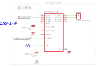
I currently have an issue with DRV8833C driver. I want to command a motor just on start stop. Therefore I am putting AINT1 at HIGH (2.7V) and AINT2 at LOW(0V) to make it turn in one sens. But no matter the voltage on AINTX, the voltage on AOUTX is equal to 1.5V. It does not vary if our small DC motor is connected or not
NSLEEP is set to HIGH and when it is at LOW level, I have 0V on all xOUTX pins, as it should be. When HIGH, all xOUTX pins are at 1.5V.

I tried to connect in parallel a DRV8833 and the later work just fine with the configuration.

Do you have any idea of what is causing this issue  and why it is working with DRV8833 and not DRV8833C even if VCP is not connected?

Kind Regards,

Sarah Duval

  • Sarah,

    With the exception of the VCP pin (existing on the DRV8833, but not on the DRV8833C), the devices are pin-to-pin compatible and feature compatible.

    Are you testing this on your own PCB or using EVMs?  Can you verify that the nFAULT pin is pulled up with an external resistor (it is an open-drain output) and what is the voltage on the nFAULT pin?  Trying to determine if the DRV8833C is in some sort of fault state.  

    The on-resistance is much higher on the DRV8833C vs. DRV8833, so potentially some sort of thermal fault could occur when driving the load, but you tested without a load, so should be OK.   

    Regards,

    Ryan

  • Hi Ryan,
    I am testing this on a custom PCB.
    nFAULT pin is driven LOW (fault) when I am applying a command on AINT1 or AINT2  (2.8V) and go back HIGH when no command are applied (0V) (even without any load on AOUT1 and AOUT2). I put a 10kOhm pull resistance between nFault pin and 2.8V.

    On AOUT1 and AOUT2 we have 0V when no command are applied and 1.5V on each when AINT1 or AINT2 or both are HIGH.

    I tested all the pins, none are connected between them. I have 16V 100nF 0603 capacitors on VINT and VM.


    Do you have any idea about what could induce such a behavior ?

    Regards,
    Sarah

  • Sarah,

    Have you tested more than one IC?  This is strange behavior to say the least.  Can you post your schematic and a screen shot of your layout?  

    Regards,

    Ryan

  • Ryan,

    Yes I have. I tested it on four PCB (one on each) on which I had the two types of packages of the DRV8833C.  Plus I connected in parallel a DRV8833 which is working perfectly even with VCP not connected.

    Bellow the schematics and a screen shot of the layout.

  • Sarah,

    Thank you for sharing the schematic.

    AISEN and BISEN need to be directly connected to GND.  Or, if current regulation is desired, they can be connected to GND via a small sense resistor.  

    Regards,

    Ryan

  • Thanks, this solve my issue. Could you just explain to me why it is mandatory to connect them to ground ? It is not for DRV8833.

  • Hi Sarah,

    Ryan is out of the office today. He will answer your question when he gets back Tuesday.

  • Sarah,

    Glad it solved the problem.  AISEN and BISEN are the ground path for the low-side FETs.  Without this connection, there can be no path for current to flow from high-side --> load --> low-side --> AISEN/BISEN (GND).  Please see the functional block diagram in the datasheet.  This is the same for DRV8833.  Somehow in your circuit with DRV8833, the current is finding some way to GND...it must.  

    Regards,

    Ryan