This thread has been locked.

If you have a related question, please click the "Ask a related question" button in the top right corner. The newly created question will be automatically linked to this question.

DRV8305-Q1: Questions

Genius 4680 points
Part Number: DRV8305-Q1
Other Parts Discussed in Thread: DRV8305, , , LAUNCHXL-F280049C

1.VCPH charge pump

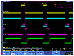
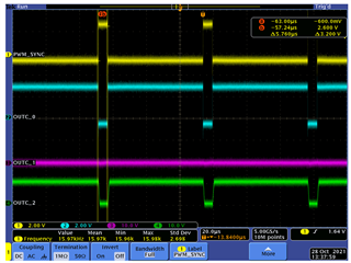
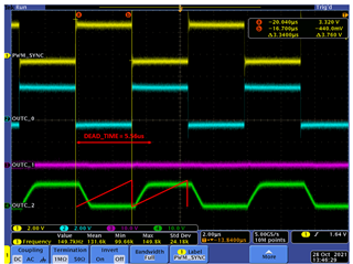
Customer would like  to know timing diagram of  "PVDD、VCPH、CP1L、CP1H、CP2L、CP2H" in tripler mode and double mode.

They would like to know how to generate PVDD+10V.

2.VVCPH_OVLO

What kind of situation is supposed, VCPH become over 14V.

3.VVCPH_UVLO2 ,VVCP_LSD_UVLO2

What kind of situation is supposed, VCPH,VCP UVLO work.

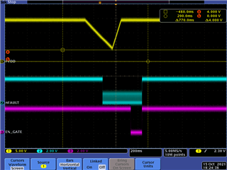
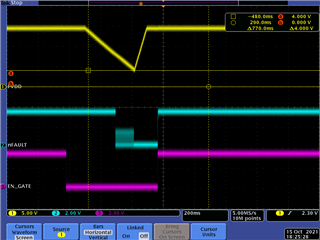
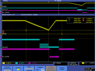
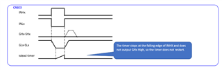
4.EN_GATE and nFAULT

When EN_GATE is always low, please let us know nFAULT pin behavior in this situation.

5.Variation of IDRIVE

Please let us know variation of  IDRIVEP_HS,IDRIVEN_HS,IDRIVEP_LS,IDRIVEN_LS.

6.VDS_OCP
Please let us know variation of  tBLANK,tVDS.

7.VDRAIN pin

Please let us know how much sink current of VDRAIN pin.

  • Hello Kura-san,

    The team is out today for the Independance Day holiday in the US. They will get back to you soon!

    Thanks,

    Matt

  • Hi Kura,

    I will get you these responses by the end of the day today. 

    Thanks,

    Aaron

  • Hi Kura-san,

    1. The DRV8305 integrates a tripler charge pump rather than many devices having a doubler charge pump, which means that the device can operate down to 4.4V because the charge pump flying capacitors (CP1, CP2) can generate up 3x the minimum voltage (4.4V*3 = 13.2V) and the charge pump controller regulates VCPH to PVDD + 10V to generate the 10-V VGS on the HS MOSFET. The integrated 10-V LDO is used to generate 10-V VGS on the LS MOSFET. 

    From 4.4-18V, the charge pump acts as a tripler and beyond 18V it acts as a doubler for better effeciency. 

    2. VCPH_OVLO is set to 14-V because there is an internal ESD diode between PVDD and VCPH rated for 15-V. If VCPH with respect to PVDD exceeds 15-V, this diode will blow up and cause a large voltage spike at PVDD. In this case, VCPH_OVLO is set to 14-V for this reason. 

    3. VCPH_UVLO2 and VCP_LSD_UVLO2 are set at the values they are in the specifications section specifically to prevent lower voltages generated from not fully conducting on MOSFETs. If the gate voltages generated from VCPH and VCP_LSD are not high enough to turn on a MSOFET at VGS=10V, then an abnormal condition has occurred, so the device will generate a fault. 

    4. When EN_GATE = LOW, the device should be in standby state and nFAULT should remain high. If a warning occurs, nFAULT will pulse for 56us high and low, and if a fault occurs, nFAULT will go low. This ppst may help: https://e2e.ti.com/support/motor-drivers-group/motor-drivers/f/motor-drivers-forum/603086/drv8305-nfault-at-startup-of-drv8305

    5. IDRIVE can vary based on PVDD, temperature, and process variation. It is more important to determine how the MOSFET switches and analyze transitions of VGS and VDS and ensuring switching times are not too fast to avoid issues such as dV/dt coupling, ringing, or shoot through current. We always recommend customers to evaluate initially at lower IDRIVE settings before switching to higher settings. 

    6. t_BLANK and t_VDS should be consistent according to internal testing and characterization data across low and high temperatures. 

    7. VDRAIN has max sink current of 2 mA. We recommend to place 100 ohm series resistor in front of VDRAIN pin.

    Thanks,
    Aaron

  • Aaron-san

    Thank you for your reply.

    Our customer has additional questions. Please check following.

    2-2) ,3-2)

    I understand the "purpose" of implementing the overvoltage protection and undervoltage protection functions, but I would like to know what kind of "situation" it works in. What are the situations in which the VCPH for P VDD exceeds 15V?

    Similarly, what are the situations below VCPH_UVLO2 and VCP_LSD_UVLO2? For example, assuming an OPEN failure of the flying condenser of the charge pump ...

    5-2)

    They are fully aware of the importance of FET switching characteristics.
    Since the gate current output by the IC has a large effect on the switching characteristics, can you provide it if there is an actual measurement value of variation?
    We would appreciate it if you could provide data with 3 patterns of maximum, minimum, and intermediate setting values.

    6-2)

    Can you provide any variation data (actual measurement value)?

    Regards,

    Kura

  • Hi Kura-san,

    2-2, 3-2)


    Voltage regulator "pumping" or "stressing" can occur for a variety of reasons on regulators or bus voltages (VCPH, VCP_LSD, PVDD, etc).

    Overvoltage

    When sinking and sourcing current at the HS and LS gates, the MOSFET gates have input capacitance and parasitic capacitance from the PCB. If the IDRIVE sink current cannot "bleed off" all of the charge at the gate during the active pulldown, then the charge gets pumped back into the regulator and can cause "voltage pumping" at VCPH or VCP_LSD, where there is more than the expected ~10V. We use overvoltage protection to ensure that:

    - The maximum voltage rating of VCP_LSD isn't violated (~20V)

    - The voltage between VCPH to PVDD does not exceed ~15V because there exists an ESD diode that will blow up and cause a large current increase at the supply if there is overvoltage on VCPH

    Note that overvoltage on VCPH could also occur if the motor acts as a generator, and the sneak path of SHx to VCPH can cause this as well (see below). 

    Undervoltage

    In general, if there is less than ~4.5V of VGS for the HS and LS gates, then this will not be enough voltage to turn on the external MOSFETs and we monitor undervoltage events so that the gate drivers shut off and indicates a fault condition before the system fails to switch MOSFETs correctly. 

    Undervoltage can also occur if inductance exists in the circuit between the recommend bypass capacitor for VM-VCP or VCP_LSD-GND and the driver IC pins. The capacitors should be placed as possible to the device, and they need to be performing at the rated capacitance. If the values are incorrect, not rated for high enough voltage, or are placed far from the device, then the capacitors may have less than 1/2 the expected capacitance and cause the regulator / charge pump circuits to not perform correctly. For instance, the VM-VCP capacitor, if less than the rated capacitance, may not be anole to store the charge pump voltage generated from the CP, and over time decrease in charge pump voltage to the point of potential VCPH_UVLO. 

    5-2) 

    Pleas see this E2E FAQ on selecting the best IDRIVE setting and why it's essential: https://e2e.ti.com/support/motor-drivers-group/motor-drivers/f/motor-drivers-forum/796378/faq-selecting-the-best-idrive-setting-and-why-this-is-essential

    6-2) 

    Variation will change depending on temperature and process variation.

    HS IDRIVE: 0.45 x TYP (MIN), 2.3 x TYP (MAX)

    LS IDRIVE: 0.45 x TYP (MIN), 2.3 x TYP (MAX)

    Thanks,
    Aaron

  • Aaron-san

    Thank you for your reply.

    Can you provide any variation data (actual measurement value) of below?

    tBLANK

    tVDS

    VDS_TRIP

    Regards,

    Kura

  • Hi Kura-san,

    I'll be out of office today, but I can reach out to the team when I come back next Tuesday for this information. 


    Thanks,
    Aaron

  • Hi Kura-san,

    All of the data we capture in the lab for each of these tests fall in-between the bounds listed on the datasheet. These parametric tests are done across temperature and voltage, so for this device that temp range is from -40C to 125C. As for the data we actually gathered in the lab we can't share that, only that we guarantee the values we measured are within DS bounds. 

    Regards,

    Michael

  • They consider to use DRV8305NEPHPRQ1.

    This part temp range is -40C to 150C.

  • Hi Kura-san,

    Is the information shared by Michael enough, or do you need further help?

    Thanks,

    Matt

  • Matt-san

    Thank you for your reply.

    Please give us your advise about following.

    about TDRIVE

    According to 7.3.5.2 and 7.3.8.2 of the data sheet, it seems that the dead time set by the DEAD_TIME bit of register address 0x7 is inserted when Vgs falls below a certain value due to the handshake.
    What is the value of Vgs when this dead time is inserted?
    They also set dead times on the MCU, but want to optimize the pre-driver settings.

    about Undervoltage

    There is word "VM-VCP" in follow description.

    Which pin is the VM? 

    -----

    Undervoltage can also occur if inductance exists in the circuit between the recommend bypass capacitor for VM-VCP or VCP_LSD-GND and the driver IC pins. The capacitors should be placed as possible to the device, and they need to be performing at the rated capacitance. If the values are incorrect, not rated for high enough voltage, or are placed far from the device, then the capacitors may have less than 1/2 the expected capacitance and cause the regulator / charge pump circuits to not perform correctly. For instance, the VM-VCP capacitor, if less than the rated capacitance, may not be anole to store the charge pump voltage generated from the CP, and over time decrease in charge pump ----voltage to the point of potential VCPH_UVLO. 

    ------

    Regards,

    kura

  • Hi Kura-san,

    Dead time for GHx and GLx begins once the DRV device ackowledges that the voltage on the gate is less than 2V - this is when the DRV8305-Q1 sees the gate as "off". Once the dead time period is over, then the other MOSFET will begin to turn on. 

    VM is PVDD in the DRV8305-Q1, older devices call the motor voltage supply "PVDD" and newer devices call it "VM". 

    Thanks,

    Aaron

  • Aaron-san

    Thank you for your reply.

    Figure9.xlsx

    Please let us know Internal resistance value between GHx-SHx and GLx-SLx.

  • Hi Kura,

    This should be 150kohm, I'll confirm today. 

    Thanks,
    Aaron

  • Aaron-san

    Thank you for your reply.

    Did you  confirm it ?

  • Hi Kura-san,

    On EVM, I measure ~275kohm resistance between GHx-SHx and ~157kohm between GLx-SNx. 

    I am confirming with design still, will get a reply by end of day today or Monday.

    Thanks,

    Aaron

  • Aaron-san

    Thank you for your reply.

    Do you have any update about resistance between GHx-SHx and between GLx-SLx ?

    And we got additional question from customer.

    DRV8305-Q1: Absolute Maximum Ratings of PVDD-VDRAIN

    According to above E2E post, PVDD-VDRAIN should be within "-10V < (Voltage difference between supply and VDRAIN(PVDD-VDRAIN)) <10V".

    Customer think that Figure24 circuit configuration in P50 of datasheet may exceed this, Will inserting a diode between PVDD and VDRAIN solve this problem?

    Regards,

    kura

  • Hi Kura-san,

    Thanks for friendly reminder. Design hasn't followed up yet so just sent a reminder. He is OoO today but I expect a reply by Monday.

    Diode from VDRAIN --> PVDD solves the issue of generator mode sourcing current from SHx to PVDD through external HS MOSFET's body diode and D(VDRAIN_PVDD) diode rather than D1, D2, and D4 of Figure 24 in datasheet.

    Thanks,
    Aaron

  • Hi Kura-san, 

    I checked with design today and confirmed that DRV8305-Q1 has 480kohm internally between HS gate to source and 360kohm internally between LS gate to source. 

    I need to re-confirm using only device or bench board as EVM likely introduced parallel impedance that was lower than the expected value confirmed with design. We will update in datasheet. 

    Thanks,

    Aaron

  • Aaron-san

    Thank you for your support.

    Please let us know more about DRV8305-Q1: Absolute Maximum Ratings of PVDD-VDRAIN

    If you connect the battery to the circuit with SW_VDRAIN open, the voltage between P VDD and VDRAIN will be 12V, exceeding 10V.

    Therefore, they think that datasheet Figure 24 and  "-10V < (Voltage difference between supply and VDRAIN(PVDD-VDRAIN)) <10V". are inconsistent.

    Please give us your advise.

    Regards,

    Kura

  • Hi Kura-san,

    I will confirm and let you know by the end of the week. 

    Thanks,
    Aaron

  • Aaron-san

    Thank you for your reply.

    Is there any update information?

  • Hello Kura-san,

    Let me confirm with Aaron and get back to you tomorrow

    Thanks,

    Matt

  • Hi Kura-san,

    I believe the image is stating that if there is a supply cutoff switch SW_VDRAIN, it should remain closed during operation so that VDRAIN always follows PVDD. Assume this switch is normally closed. If SW_VDRAIN is open, the battery is still connected and Generator Mode (large increase in SHx, or many volts above PVDD) so that the diode D_VDRAIN_PVDD can be used to flow current back to the supply rather than internally through the body diodes and ESD diode (that would fail). 

    Regardless, the battery should always remain connected with the switch normally closed so that PVDD = VDRAIN. The battery should not be connected when the switch is open, or else you will violate the -10 to 10V max rating of PVDD-VDRAIN voltage difference. 

    Thanks,
    Aaron

  • Aaron-san

    Thank you for your support.

    We got additional question from customer.

    About ± 10V of PVDD-VDRAIN
    When V (P VDD) -V (VDRAIN) <-10V, it is expected to be a problem because a current path is created by the diode inside the IC as in the generator mode.
    However, when V (P VDD) -V (VDRAIN)> + 10V
    They don't know what the problem is.

    Please specify the internal circuit and explain what happens when it exceeds + 10V.
    (By the way, the rated value is not found in the data sheet of DRV8305-Q1.)

    Please give us some advice

    Regards,

    Kura

  • Hello Kura-san,

    When PVDD is greater than VDRAIN, the VCP voltage will be much larger than VDRAIN + 10V.  This results in drawing excessive current through the VGS clamp (i.e. see figure 9 in the datasheet) when trying to turn the high-side MOSFET ON.

    For example, if PVDD is 22V & VDRAIN is 12V, VCPH will be nominally 32V. When trying to turn on the high-side MOSFET, the charge pump voltage is 32V but the MOSFET source will only be 12V (VDRAIN). The gate to source clamp internal to the DRV8305 will limit the voltage to protect the external MOSFET gate but it will dissipate extra power when turning the high-side MOSFET ON.

    This will cause more power dissipation and may cause damage if the voltage delta is very high.

    Thanks,

    Matt

  • Matt-san

    Thank you for your support.

    Is there any problem if EN_GATE is set to Lo when PVDD is VDRAIN+10V or higher?

    The charge pump operates by setting EN_GATE to Hi.
    So customer think they can avoid the phenomenon in your answer by setting EN_GATE to Lo.

    Please give us your advice.

    Regards,

    Kura

  • Hello Kura-san,

    This issue is avoided if the driver is in sleep mode by taking EN_GATE low.

    Thanks,

    Matt

  • Matt-san

    Thank you for your support.

    We got additional question from customer.

    When PVDD is VDRAIN + 10V or higher, is there any problem if EN_GATE = Hi but INH_x = Lo?

    When INH_x = Lo, the potential difference between GH_x and SH_x is 0V, so they think they can avoid this problem.

    Please give us your advice.

    Regards,

    Kura

  • Hi Kura-san, 

    This should also avoid the issue as well by taking INH_x = Low since the high-side MOSFET's VGS voltage = 0V in that state. 

    Thanks,
    Aaron

  • Aaron-san

    Thank you for your support.

    We got additional question from customer.

    About low voltage of PVDD
    When PVDD drops and recovers without falling below PVDD_UVLO1 (see the picture below)

    case.xlsx
    Will the IC return like CASE1? Or is it still stopped like CASE2?
    This is a Fault type error, so they expect it to be CASE2.

    Regards,

    Kura

  • Hi Kura-san,

    nFAULT should latch low once PVDD < PVDD_UVLO2 (Case 2). You will need to issue a reset pulse on EN_GATE or set the CLR_FLTS bit to clear the fault and make it go high again. I have confirmed this on the DRV8305-Q1EVM. 

    Thanks,
    Aaron

  • Hello Kura-san,

    Do you need any additional help on this thread?

    Thanks,

    Matt

  • Matt-san

    Thank you for your support.

    We got additional questions from customer.

    Please see attached.

    expected waveform.xlsx

    1.About the variation of dead time:
    The dead time is that the time of td_min + tdtp is inserted after the handshake.
    What is the variation of tdtp of td_min?
    What is the variation of tdtp?
    If the guaranteed value cannot be provided, the measured value, design value, or theoretical value may be used.

    2.About the behavior when the falling edge of INHx is input during the dead time:
    When inserting the dead time, the timer is operating inside the IC they guess.

    If the falling edge of INHx is input during the dead time, it is expected that the following CASE1 or CASE2 operations will be performed.
    Which CASE will work? Or do you do something else?
    CASE1:
    The timer counts up to the set value and restarts immediately.
    CASE2:
    The timer restarts immediately after inputting INHx.

    In this case, it is expected that the upper gate (GHx) will not be output.

    Please advise us.

    Regards,

    Kura

  • Hi Kura-san,

    These are good questions, I'll have to confer with design team to determine "how" the dead time timer works since there is a lot of internal handshaking happening. My guess is Case 2 for when duty cycle > 91%, which means the dead time timer prioritizes INHx falling edge over dead time timer completing the period.

    I also do not expect any variation from the timer, but I'll ask as well how much variation can occur if known. I'm assuming any variation in the tuning of the system clock will determine any variation of the dead time timer.

    Finally, I'd like to point out that dead time occurs twice: 

    1) between when GLx goes low and GHx goes high

    2) between when GHx goes low and GLx goes high

    For a PWM period of 62.5us, this means that the amount of dead time expected is 2*(td_min + tdtp) = 2*(5280ns+280ns) = 11.12us. This means the largest duty cycle achieved for 16kHz is 82.2% before dead time insertion affects the GHx output.

    What is the minimum duty cycle resolution needed for your application? I would calculate the DT setting based off this spec. 

    Thanks,
    Aaron

  • Aaron-san

    Thank you for your support.

    I got following answer from customer. 

    >What is the minimum duty cycle resolution needed for your application? 

    ---->Since the MCU operates at 20MHz, the resolution will be 50ns. If you need any other information please let us know it.

    Customer asked about your comment " I would calculate the DT setting based off this spec."

    Our understanding is you will prepare the answers to the following questions.(Is our understanding correct ?)

    This question is caused by the fact that the pre-driver setting value is only the typ value...

    1.About the variation of dead time:
    The dead time is that the time of td_min + tdtp is inserted after the handshake.
    What is the variation of tdtp of td_min?
    What is the variation of tdtp?
    If the guaranteed value cannot be provided, the measured value, design value, or theoretical value may be used.

    Regards,

    Kura

  • Hi Kura-san,

    I looked at characterization data of t_dtp and found that t_dtp varies based on the DEAD_TIME setting, VM, and temperature.

    Can you please share what DEAD_TIME setting is to be used, ambient temperature, and VM of the application is so I can summarize the variation of dead time (t_dtp)?

    I am confirming with design the variation of td_min. 

    Thanks,

    Aaron

  •  Aaron-san

    DEAD_TIME setting is to be used

    ->Customer think the 0x7 register setting is  3.52us (b110) or 5.28us (b111).

    ambient temperature

    ->The temperature around the IC is -40 to + 125C

    VM of the application

    ->6V to 18V

    Regards,

    Kura

  • Hi Kura-san,

    For DEAD_TIME = b110:

    Variation of dead time across VM = 6-18V is 3.739us (-41C) to 3.770us (123C)


    For DEAD_TIME = b111:

    Variation of dead time across VM = 6-18V is 5.487us (-41C) to 5.533us (123C)

    This dead time setting includes the minimum dead time (280ns). Still awaiting confirmation of whether that varies or not depending on handshaking of the gate drive state machine. 

    Thanks,

    Aaron

  • Aaron-san

    Thank you for your answer.

    It seems that the answer is only on the Min side, so customer would like you to answer the variation on the Max side as well.

    If you can provide information of  the variation on the Max side, please let us know it. 

    Depending on the operation of the gate drive state machine, the static characteristics of the motor due to the dead time,

    It affects the dynamic characteristics not a little, so they would like to confirm it.

    Also, you are considering the operation of the gate drive state machine, but is it okay to think that it will not behave like CASE3 in the attached Excel?

    waveform.xlsx

    Regards,

    Kura

  • Hi Kura-san,

    I have talked to the design team and they confirmed in the DRV8305-Q1 that the dead time implementation is digital, so the maximum variation is +/-10% of the typical specification for td_min and for tdtp across temperature and process variation, not so much motor voltage. 

    So td_min can vary by +/-28ns, and tdtp can vary up +/- 528ns (when DEAD_TIME = 5280ns). 

    I need to confirm with the designer who designed the dead time timer in this part how the prioritization works so Case 3 is not possible. Please let me provide a follow up once I can confirm the dead time timer behavior. 

    Thanks,
    Aaron

  • HI Kura-san,

    Design said it may take some time to gather that data. Let me run a bench test with the DRV8305-Q1EVM board tomorrow to see what output occurs at GHx/GLx to confirm whether Case 1/Case 2 occurs or Case 3 occurs. 

    Thanks,
    Aaron

  • Aaron-san

    Thank you for your continued support.

    We got a new question from them.


    About EN_GATE and nFAULT:

    The behavior of nFAULT with respect to P VDD voltage and EN_GATE is assumed to be patterns A, B, and C below. Is this assumption correct?

    PVDD EN_GATE nFAULT.xlsx

    If their assumptions are incorrect, please tell us the correct behavior of nFAULT.

    regards,

    Kura

  • Hi Kura-san,

    Those assumptions should be correct as long as nFAULT goes high as soon as EN_GATE = high. The device needs 1ms to fully turn on the gate drive supplies, but I don't believe nFAULT should toggle if its above PVDD_UVLO2.

    I did not have time to check in the lab yesterday, let me run yesterday's and today's tests and share data with you on the waveforms.

    Thanks,
    Aaron

  • Hi Kura-san,

    I took these captures in the lab today to resemble the timings of PVDD and EN_GATE. I tried to ensure that PVDD did not dip below PVDD_UVLO1

    Pattern A: 


    Pattern B:


    Pattern C:


    As far as capturing GH_A and GL_A with dead time = 5280ns, I have to rerun the test on Monday so I can write to it with SPI using the EVM. 

    Thank you,
    Aaron

  • Aaron-san

    Thank you for your continued support.

    Please let me know if there is any update of waveform and dead time information.

    Regards,

    Kura

  • Hi Kura-san,

    I talked about the waveform with my manager and he believes that Case 3 may occur because the DRV8305 will prioritize the inputs over the dead time timer, so the dead time timer restarts. Since GHx never goes high, it will ignore outputting GHx as the INHx signal is already low at that point.


    In order to confirm on bench, my plan is to interface the BOOSTXL-DRV8305 with the LAUNCHXL-F280049C with custom software that can provide PWM signals and a SPI interface to set the dead time. I ordered a BOOSTXL-DRV8305 since I could not find one in the lab. Once I receive it, I will set the dead time setting myself and run the exact test case shown above to confirm if that is the behavior. This will take about a week if that is okay.

    Thanks,
    Aaron

  • Hi Kura-san, 

    I tested the waveforms to confirm behavior of the DRV8305 and try to understand the behavior of the Dead Time timer. 

    Setting DEAD_TIME = 5280ns, PWM freq = 16kHz, changing INHA/INLA duty cycles
    Ch 1 = INHA
    Ch 2 = INLA
    Ch 3 = GHA
    Ch 4 = GLA

    HS/LS = 15%/85% - dead time timer ends when input changes. Not sure if DT timer stops or restarts. We see ~5560ns of dead time (DT + DT_min)

    HS/LS = 9%/91% - VGSH doesn't turn on because dead time > PWM "on" time. Dead time timer either stops or continues at INHx falling edge. 

    If dead time timer stops (Case 3), then we should see a INHx cause an output at GHx after the INLX = falling edge dead time timer period expires (5560ns). Best way to confirm this is to dramatically increase PWM frequency (~150kHz) and switch at 50% to see GHx behavior after 5560ns from INLx falling edge. If no output is seen at GHx, then we know the dead time timer restarted (Case 2) since "ON" period is less than DEAD_TIME.

    Test case above shows Case 2 behavior is occurring. After INLA has falling edge, dead time timer starts, so GHA never outputs. 

    After INHA falling edge, dead timer restarts and we still don't see GHA output when INHA goes high again because dead time timer is restarted. 


    Thanks,
    Aaron

  • Aaron-san

    Thank you for your support.

    We got new questions from customer.

    waveforms.xlsx

    Question1:

    About Pulse input to EN_GATE:

    If something goes wrong and nFAULT is latched low, EN_GATE will be reset by inputting a Low pulse, but if it still does not recover, they are thinking of

    inputting a Low pulse again.

    In that case, the pulse will be like the one attached(Please see "nFAULT&EN_GATE" sheet), but is there any problem?

    Is it okay to input a pulse of Hi = 2ms, Lo = 2ms to EN_GATE?

    Question2:

    About the starting point of tBLANK:

    Where does the tBLANK timer start when INH and INL are entered as shown in the figure(Please see "INHx_INLx_GHx_GLx" sheet)?

    They expect to start with one of A, B, or C.

    Regards,

    Kura

  • Hi Kura-san,

    I will provide a more formalized response tomorrow during business hours. 

    Thanks,
    aaron