This thread has been locked.

If you have a related question, please click the "Ask a related question" button in the top right corner. The newly created question will be automatically linked to this question.

DRV8350S-EVM: DRV8350S-EVM

Part Number: DRV8350S-EVM
Other Parts Discussed in Thread: CSD19535KCS, DRV8350

I am trying to develop a 1.2Kw motor driver fir that I ordered one drv8350s evm 

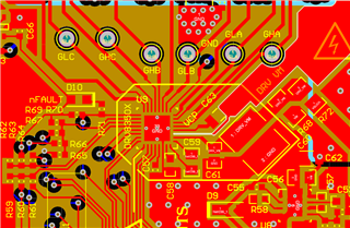
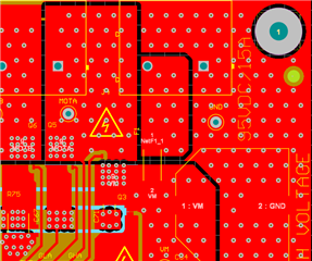
Today I recived my drv8350s evm and then I start running the board using example code as per ti web side and for control using the pc application downloaded from ti web site.

Motor voltage = 60v

Current is approx 2 amps

6x pwm mode 

Sensored control 

Motor start spining and suddenly I change the direction and then I got gate drv fault.

Tried lot of times to clear the fault using spi as well power off the board for 10 min but every time I enable the gate driver its showing gate drv fault, specifically on Phase C low side 

All gate drv Current and other setting are default as in example code

Please guide me for next steps for debugging

Also it will be great help if you can provide me state machine diagram for drv8350s sensored based motor control firmware 

Thanks in advance 

  1. Saikat jana
  • Hello Saikat,

    We will get back to you on Monday!

    Thanks,

    Matt

  • Thanks for look into it 

  • Will wait for your kind support 

  • Hi Saikat,

    I am sorry to hear about the issues you are facing. Would you be able to check the IDRIVE settings that are found in the Gate Drive HS and Gate Drive LS registers? I am thinking that the DRV8350S GUI defaults to the default setting of the DRV8350S device (which is max IDRIVE, 1000mA/2000mA for IDRIVE_P/IDRIVE_N). If that is the case then the IDRIVE settings need to be reduced to the lowest IDRIVE setting (50mA/100mA) based on the Qgd of the MOSFETs on the EVM. This lower IDRIVE setting will allow for operation where the gate drive current is not high enough to cause damage due to ringing during switching events. If the EVM operates at too high of an IDRIVE, then that can result in access ringing during MOSFET switching, which could damage the driver due to an abs max violation that occurs from the amplitude of the ringing. If the driver is damaged, this could prevent one of the MOSFETs from fully turning on which will trigger a gate drive fault. Unfortunately I suspect that this could be the case with your EVM.

    Regards,

    Anthony Lodi

  • I checked all the the I drive high and low setting and it looks like normal not too high 

  • I Drive is arround 150mA source and 300mA sink and fault still present. Did I damaged the gate driver. But its commucating with mcu

  • Hi Saikat,

    Was that IDRIVE setting of 150mA/300mA the default setting that the driver was using when the damage occurred? Or did you change it to 150mA/300mA at a later point in time? The Qgd of the MOSFET is quite low, so even the default was 150mA/300mA, it is still possible that there was a transient that caused damage to the driver. For the fault are you getting a GDF fault for Fault Status 1 and a VGS_LC error under the VGS Status 2? If that is the case, then that is being caused because the gate to source voltage on the low side MOSFET is not being enhanced when it is supposed to, and points to the DRV being damaged near the low side Gate of phase C which is preventing the voltage from being fully applied to the low side gate. You would still be able to communicate with the MCU, but would get a fault any time you try to commutate the motor. It is possible that the MOSFET could be damaged instead of the driver, but that is not as likely.

    With the device off, you can take resistance measurements for the GLC to ground, SLC pin to ground, and between GLC and SLC and then compare it with the pins of a non damaged phase to see if  there is any differences in the resistance of these pins that may indicate damage.

    Regards,

    Anthony Lodi

  • All mosfet are showing same resistance 

  • DRV8350S Is little hot while motor is not running or I am not able to run motor after the fault. I think gate driver got damaged and unfortunately all ic are out of stock 

  • Hello Saikat,

    Anthony is out of office until Thursday. 

    Can you show a table of the actual resistance measured from each pin for both the non-functional unit and known good unit?

    Thanks,

    Matt

  • I am able to run the motor again 
    DRV8350S got damaged I changed that and start working 

  • My Motor Spec is 

    1000 Watt 

    Voltage - 60V

    Please suggest to me, How to select the PWM Frequency and also which current sensing method is good and how to select that

  • Hello Saikat,

    I am glad you were able to run the motor again. Typically you can use PWM frequency of 20kHz, using someting lesser will be in an audible frequency range. The frequency mainly depends on the L/R of your motor, this will give you the minimum PWM frequency, the other item that comes into play are FETs you are using limited by how quickly they can turn on and off. If you are using a low inductance motor then a higher PWM signal can be used, please refer to this previous post for the formula that was used.

    For current sensing methods we have a Texas Instruments Precision Labs video with references you can watch at this link: https://training.ti.com/ti-precision-labs-motor-drivers-current-regulation?context=1139747-1138777-1139743-1148013 

    I hope this helps!

    Best,

    Isaac

  • Hi Today I measured the Phase PWM and was surprised, I configure the time for 25Khz frequency but in the output the PWM Frequency is 20Khz 

    Is device limit the frequency to 20Khz ??

  • Hello Saikat,

    The device spec limit on DRV8350S for the applied PWM is 200kHz, so there should be no problem running 25kHz. Did you measure 20kHz at one of the INHx or INLx pins?

    Best,

    Isaac

  • Hi 
    I did more testing on EVM Board and I am able to understand all the frequency-related things.

    But there are lots of problems in the EVM Board and it damage 4 DRV8350S IC and Now I am scared because I only have left 2 new in my stock

  • My Gate Current Settings are - 

    IDRIVEP_HS - 0010b = 100 mA
    IDRIVEN_HS - 0010b = 200 mA

    IDRIVEP_LS - 0010b = 100 mA
    IDRIVEN_LS - 0010b = 200 mA

    TDRIVE - 00

    DEAD_TIME - 00b = 50-ns dead time

    The problem occurs only when I reached more than 90% Duty Cycle 

    My Motor Parameter and Supply Voltage-

    48V DC - 750W  3 Phase E-Cycle Motor (Chinese One, No Datasheet)

    Supply Voltage - 60V DC

  • Also, Notice some Points if I go with Lowest Setting everything working fine but frequently getting VDS_OCP at 90 - 95% Duty Cycle

    I am also checking the datasheet but not understand properly some calculations on page number 68 and 69 the I drive calculation, why Tr and Tf is selected 100ns to 300ns 

    Please suggest to me How to select Trdive and Dead Time 

    My Motor is running at 25Khz and total current consumption approx 2Amps as per shunt Resistor connected in EVM Board 

  • Hello Saikat,

    Glad to hear that you got all the frequency related things down. I am sorry to hear that you have gone through a couple of units. I will give you a quick breakdown of how we calculate or set some of the parameters you have listed here.

    IDRIVEP and IDRVEN are calculated using the formula Q_gd/tr and Q_gd/tf respectively, the values for Tr and Tf on the datasheet are selected to typical values that are a good rule of thumb to generally follow. Having lower values typically causes switching loss and having values above the rule of thumb generally can be too fast causing transients that could damage your device. So these values are pretty good rule to follow when calculating for your I drive values. Q_gd can typically be obtained from your MOSFETs data sheet.

    TDRIVE is the duration in which your current setting will be delivered to the MOSFET. This can be set to the max without any sort of issues, typically you want it to be at least 10xTr and 10xTf.

    DEAD_TIME- is the amount of time between each phase is turned on to make sure theyre not on at the same time. 100 ns is the recommended setting for this but 50ns should not be an issue.

    VDS_OCP depends on the VDS_LVL setting, perhaps going to the next setting will prevent you from hitting VDS_OCP.

    Is there a specific reason why 60V supply is used for a 48V motor?

    Best,

    Isaac

  • We are trying to develop Motor Driver for Small Scale EV and the EV uses 14S Li-ion Battery and the max Battery voltage 58.8 Volt 

  • Tr and Tf as per Mosfet Datasheet (CSD19535KCS)are 

    Tr - 15ns
    Tf - 5ns

    But The calculation is based on 100 to 300 ns. for IDRIVEP and 50 to 150ns for IDRIVEN why it these values are selected related to on time and off time.

    In DRV8350 There are 2 sets of register IDRIVEP_HS and IDRIVEP_LS (Same for IDRIVEN ) will the values be same in both.

    My motor has no load on it  and I don't know why this VDS_OCP faults are raised as per setting my  VDS_LVL  is 0.6V and my as per EVM board VDS_OCP fault is supposed to come when we draw more than 55Amps but we are drawing only 2 Amps 

    It will be a great help if you can suggest to me some debugging techniques so that I can analyze the problem on my end  

  • Every time when DRV8350 got damaged I Got gate drive fault in Low side C chanel 

  • Hello Saikat,

    I am currently out of the office and will not be back until Tuesday due to a holiday in the US. I will provide a response to your questions then thank you for your patience.

    Best,

    Isaac

  • Hello Saikat,

    Thank you for your patience. As mentioned the values of 100-300ns for IDRIVEP and 50-150ns for IDRIVEN were chosen because these are typically values that work well in most systems.

    For the VDS_OCP fault if you are switching too fast you might be experience shoot-through which might cause the system to see above the 55A threshold from a 60V source.

    I highly recommend reading the following document : High-Power Design Through MOSFETs and MOSFET Gate Current (IDRIVE) section 3 has good info on setting IDRIVE and section 6 has info on shoot-through.

    Were you able to collect any waveforms when the device gets damaged? Such as Low Side C. That might be extremely useful in identifying the problem.

    Best,

    Isaac

  • Hey Saikat,

    I forgot to comment on the values used for IDRIVEP_HSIDRIVEP_LS, IDRIVEN_HS and IDRIVEN_LS. The same formula is used to calculate these values, and you will use the same value across all 3 high side and low side MOSFETs. So, be sure to still use the recommended formula based on Q_gd/t_rise/t_fall then you can chose the nearest setting.

    Best,

    Isaac

    • Thanks for the information. As I previously faced my gate driver ic again damaged and exactly on low side c phase and I don't have any extra ic with me. I have wait for new ic to come.
  • I will complete my PCB layout and order the new board because evm dose not have all necessary protection so it's causing damage. Please wait until I got my new board and driver ics 

  • Hello Saikat,

    Thanks for the info. Sorry to hear about the troubles with the EVM. Feel free to reach out if you are still having issues on your board or if you have other questions.

    Best,

    Isaac

  • Hi 

    Sorry for the late response. Today I completed my Circuit Design and PCB design and now gerbers are ready for order but before move forward, it will be a great help if you can verify my Schematic and PCB layout and let me know your thoughts on that 

    Waiting for your valuable reply 7870.Top.pdfL4-BTM.pdf1768.Schematic.pdfL-2-VCC.pdfL3-GND.pdf

    Saikat

  • Hello Saikat,

    No worries, glad that you were able to make some progress on your end. I will set up a review with the team to review your schematic and board layout. I should be able to get you any feedback by no later than Wednesday. Thank you for the files and your patience!

    Best,

    Isaac

  • Hello Saikat,

    The schematics you posted did not have values on the components, so I will not be able to comment on values selected but overall the notes were on the layout and not so much on the schematic. I will post the notes tomorrow, thank you for your patience!

    Best,

    Isaac

  • Please find the schematic with all the values.

    Some Components of the Schematic don't have the value like in the RC snubber circuit, Without testing, I am not able to calculate the value for R and C and I need help on selecting TVS Diode for the Gate of Mosfet. 

    TVS Diode Ref Number - D3,D5,D12,D13,D14,D15

    One of the biggest problems is the IC is totally out of stock on Mouser and other vendors web site.
    It will be a great help if you can provide some R&D Quantity around 20 Pcs (We will buy that as per market price )so that we can start our testing at least 

    Thanks for your support

    SchematicWithValue.pdf

  • Hey Saikat,

    Thanks for the schematic with the values I will review them shortly. 

    For the RC Snubber circuit we have an FAQ you can reference to help you select the best values for this: https://e2e.ti.com/support/motor-drivers-group/motor-drivers/f/motor-drivers-forum/991693/faq-proper-rc-snubber-design-for-motor-drivers?tisearch=e2e-sitesearch&keymatch=RC%20snubber%20faq#

    Let me review with the team to see if we have any devices that we can provide to you.

    Best,

    Isaac

  • Hello Saikat,

    Attached you can find the notes on the schematic and layout:

    Schematic & Layout Review Notes.docx

    It might be helpful to review our app note on best layout practices for a motor driver, it contains more information on some of the notes I provided in the document above: https://www.ti.com/lit/an/slva959a/slva959a.pdf

    Thank you for providing values on your schematic, I did not find any areas of concern as far as the values selected went. I hope the FAQ on the RC snubber will help you determine values for that portion of your circuit. As far as TVS diodes we typically do not help customers select these, but I did find an app note that might be helpful in your search for some diodes: https://www.ti.com/lit/an/slvae37/slvae37.pdf 

    I hope this helps!

    Best,

    Isaac

  • Hello Saikat, 

    I have sent you a friend request via E2E if you could please accept. Thank you!

    Best,

    Isaac

  • Hi 

    Thanks for the great update and suggestions. Please find the reply for the layout notes. 

    I have already gone through the e2e thread for RC Snubber component selection and I will select after we receive our PCB and I will let you know if I faced any issues on that.

    If we do not get this IC from any vendor or your side we need to change our design because we already have orders in our pipeline and we need supply the products to our customers. 

    Please help us inSchematic & Layout Review Notes-Reply.docx procuring this IC.

  • Hi 

    Thanks for the great update and suggestions. Please find the reply for the layout notes. 

    I have already gone through the e2e thread for RC Snubber component selection and I will select after we receive our PCB and I will let you know if I faced any issues on that.

    If we do not get this IC from any vendor or your side we need to change our design because we already have orders in our pipeline and we need supply the products to our customers. 

    Please help us in procuring this IC.

    Thanks for your support

    4527.Schematic & Layout Review Notes-Reply.docx

  • Hello Saikat,

    I have sent you a private message regarding the IC so we will continue those conversations through those messages.

    Q: There are 2 Option available for VM Pin of DRV8350 – We can Connect V-Motor net to VM pin which will have 60V or We can connect 12 Volt regulated Output and as our design and EVM design have the 12v regulator and the 12v regulator only capable to deliver 350mA so why we need increase trace width is not clear to me. 

    • Regarding the comments on the PCB layout, if you are using a 12V regulator with 350mA the 20 mil trace should work well, the comment I made also included restructuring some of these connections. The VDRAIN path is somewhat long which can introduce parasitic inductance in itself. Rerouting this as a short and direct trace could help reduce any parasitic inductance. 
    • For example: On the EVM we have VDRAIN connecting directly to VM via a polygon pour. I know you have a 0 ohm resistor on yours but something similar would help reduce the trace length.


    Q: Can we pour with ground and use multiple via for stitching and should we add pouring in every layer?

    • This connects to my previous answer but yes you can pour with ground and stitch them through layers of PCB. I am not sure which PCB design tool you are using but some of them have auto stitching features, I usually feel like it does not add enough so you can always go in manually and add more stitching vias. Here is an example of our board:


    • We typically do have pours in every layer, whether it is a ground, VM, or other signal pours can vary. Here is an example of the different ground pours between some layers on the DRV8350 EVM.


    Here is the download link for the EVM files if you need more examples: https://www.ti.com/lit/zip/slvc763

    Best,

    Isaac

  • Hi 

    We received our PCB and all the components. Today I assembled the PCB. We will start the testing very soon  

  • Hey Saikat,

    Thanks for the update! Let me know if you have any other additional questions, if you do lets start another thread since we try to keep the threads at one question per thread to make solutions easier to find.

    Best,

    Isaac