This thread has been locked.

If you have a related question, please click the "Ask a related question" button in the top right corner. The newly created question will be automatically linked to this question.

DRV8844: Current sense, max voltage on SRC12/34

Part Number: DRV8844
Other Parts Discussed in Thread: DRV8251A

Hello, drv8844_9v_out12short_1rshunt.png

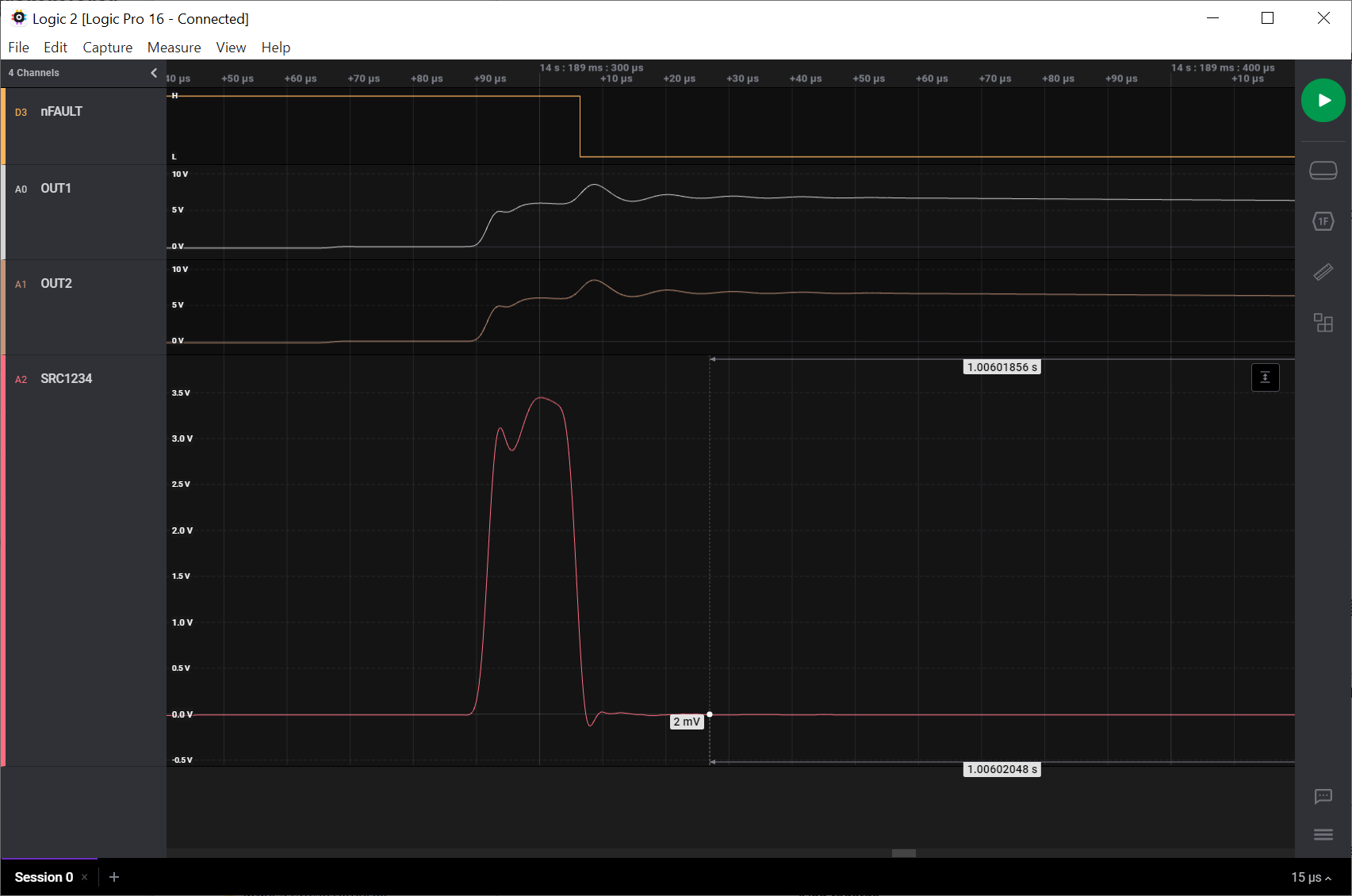
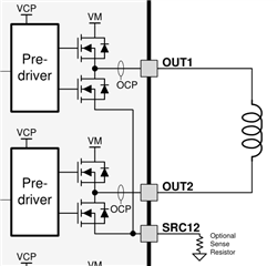
I am designing a control board for bistable water valves operated at ~9V. I'd like to control the on/off solenoid current bursts (300mA for 250ms resp. -50mA for 60ms) and to detect various abnormal conditions including valve presence and shorted terminals. To simplify the design I was planning to use a 1R shunt resistor and to deliver the SRC12/34 voltage (via 1k) to the ADC input of the uC (which offers a VREF of 1.1V and allows a max voltage of 5V).

Now, shorting the terminals I observe that the voltage at SRC12/34 rises to 3.5V for 15us and that then the overcurrent protection of the DRV8844 kicks in, shutting down the FETs.

But according to the datasheet the max voltage at SRC12/34 is +-0.6V. This datasheet max voltage requires me to use a much smaller shunt resistor e.g. 0R1, and therefore limits my ability monitor with the uC the inductive current rise (in order to detect the solenoid presence) in this simple way. Rather I would probably have to add some OPA amplification of the SRC12/34 signal on the board, adding quite a bit of noise.

Now, I was assuming that the max +-0.6V versus VNEG indicates that the FET source is protected from ESD by some clamping diodes. But according to my measurements the voltage *does* rise to 3.5V at SRC12/34 when shorting the terminals. How can that be?

So my question basically boils down to: What happens if I exceed the 0.6V on SRC12/34? Which components in the IC are stressed by this voltage and how much? And would it be OK if this happens only rarely and shortly?

Kind regards,
Sebastian

  • Hi Sebastian,

    Now, I was assuming that the max +-0.6V versus VNEG indicates that the FET source is protected from ESD by some clamping diodes. But according to my measurements the voltage *does* rise to 3.5V at SRC12/34 when shorting the terminals. How can that be?

    The SRC pins are connected directly to the source pins of both low-side FETs. The voltage from the SRC with respect to the device GND (VNEG) needs to be +-0.6V. In the case of a short or a large inrush current, the current through the H-bridge can cause the the SRC voltage to go above 0.6V which can prevent the low-side FETs from turning ON. When you short the terminals, the current will rise very quickly (it seems like it is 3.5A based on the 3.5V in SRC pins). Afterwards, the device will shutdown due to overcurrent. There is no actual clamp in the SRC pin.

    So my question basically boils down to: What happens if I exceed the 0.6V on SRC12/34? Which components in the IC are stressed by this voltage and how much? And would it be OK if this happens only rarely and shortly?

    One things that could happen is the VGS of the LOW-side FETs may not be enough to fully enhance and turn ON the FETs. This will cause the H-bridge to be in an abnormal state where only the HIGH-side FETs can be turn-on.

    My recommendation is to select a sense resistor low enough to ensure the SRC voltage is always less than 0.6V even in an overcurrent event.

    Alternatively, you can take a look at the DRV8251A driver which comes with an integrated current sense amplifier which outputs a voltage proportional to the load current. So there will be no need for a big sense resistor or an amplifier.

  • Thanks Pablo for that clarification. Good to know that there is no clamping and that SRC12/34 overvoltage due to a "big" current sense shunt would only reduce the Vgs of the low-side FET, potentially to the point of the FET starting to shut off (thereby reducing the overcurrent again and thus with a risk of the IC missing an overcurrent fault event).

    I take note of your recommendation. But if I'm not mistaken the typical overcurrent protection trip level of the DRV8844 is 5A, so with a chance of a short between outputs and a 10uF cap between VM and VNEG able to deliver those 5A this implies that the biggest shunt resistor you could use with the DRV8844 is 0R1, implying quite some noise in particular at lower currents.

    I guess I can measure at which source voltage above VNEG the low-side FET starts of close; that should give me some information about the additional maneuvering space I have beyond the safe 0.6V value of the datasheet for the shunt resistor value selection.

    The DRV8251A does not suit my application unfortunately. I plan to control 13 valves using four DRV8844 where never two valves are switched at the same time. Also to save cable wires I will therefore connect one side of all solenoids together to one OUT1, and the 13 other sides are then spread over the other 15 OUTn. To switch on valve i OUT1 goes VNEG, OUTi goes VM and all other OUTx stay Z, and to switch off valve i OUT1 goes VM, OUTi goes VNEG and all other OUTx stay Z. This scheme requires multiple half-H bridges where H, L and Z of all outputs are individually controllable, and there are not so many of those out there ...

    Kind regards,
    Sebastian

  • Ok, I did a few tests of the DRV8844. Setup was +9V - 4 - 11, 14 - 19 - 28 - GND, 15 - 16 - 17 - 26 (no SLEEP, no RESET, EN1 high, all IN and all other EN low), 6 - 9 - 10Ω - GND, the required capacitors between 1/2, 3/4, 11/14 and 14/15, and another test bench supply between 5 (OUT1) and VNEG/GND. I selected a few voltages to feed into OUT1 and measured the voltage between SRC12 and VNEG/GND, the current into OUT1 and, at higher voltages into OUT1, the temperature of the DRV8844 (using a FLIR). I also calculated the current out of SRC12 using the known shunt resistor value, and derived the Rds of the low-side FET from that current and the voltage difference between OUT1 and SRC12:

    OUT1 SRC12 Vds Iout1 T8844 Isrc12 Rds
    [V] [V] [mV] [mA] [°C] [mA] [Ω]
    0.5 0.49 12 49 49 0.24
    1.0 0.97 31 98 97 0.32
    1.3 1.26 38 134 126 0.30
    1.6 1.55 49 173 155 0.32
    2.0 1.88 110 352 39 188 0.59
    2.3 2.05 247 640 75 205 1.20
    2.4 2.10 300 731 90 210 1.43

    Now, I can't fully explain those measurements. Lower voltages are fine, but as from 1.6V the current into OUT1 seems not to return only out of SRC12 anymore but rather to find another path towards VNEG/GND, bypassing my current measurement shunt resistor?

    I'm only a hobbyist, so please take all of this with a grain of salt and a big margin for mistakes on my behalf, but possibly there is some explanation?

    Kind regards,
    Sebastian

  • Sabastian,

    Pablo is on leave until Friday.  He can respond then.  

    Regards,

    Ryan

  • Hi Sebastian,

    One thing I noticed in your data is that the RDSon calculations are not correct. You can calculate the RDSon by dividing VDS and IOUT1 (VDS/IOUT1). How are you doing this calculation?

    I graphed IOUT1 (x-axis) and VDS (y-axis). You can see that the slope is fairly linear and it's close to the specified RDSon values on the datasheet.

    For this test, was the device enabled? nSLEEP=1?

  • Hi Pablo,

    thanks for your reply. Let's ignore the Rds column in my table for now, and let me formulate my confusion differently.

    In my measurements, when I apply 2.4V between OUT1 and VNEG, with a 10R resistor between SRC12 and VNEG, I observe 731mA flowing into OUT1 and 2.1V at SRC12. But 2.1V at SRC12 implies that only 210mA are flowing out of SRC12 and through my 10R to VNEG.

    So how do the remaining 521mA entering OUT1 flow through the DRV8844 bypassing SRC12 to VNEG?

    I mean, either this current passes as well through the low-side FET but then bypasses somehow SRC12 and goes via a less-resistent path than 10R to VNEG (and this case is depicted in your chart), or else it bypasses somehow both the low-side FET and SRC12 going to VNEG (and this is the speculative assumption I made for my Rds calculation in the table above).

    Of course we are outside of datasheet spec realm here, with SRC12 way above the ±0.6V maximum rating. Still it would be quite interesting to understand what is going on here that is not visible in the functional block diagram.

    Kind regards,
    Sebastian

    PS: Yes, nSLEEP(17) was connected to V3P3OUT(15) in my measurements, so when I wrote "no SLEEP" in my list of connections and components used for the test bed above I meant nSLEEP=1.

  • Wangnick,

    Thank for the clarification and extra information. I will have to take a closer look at the device to see if there is another path. This will take some time so please give me about 2 days to get back to you.

  • Hi Wangnick,

    I have not been able to get the information. In the meantime, can you do another experiment:

    • use similar set-up as you did previously but replace SENSE resistor with lower resistance (<500mΩ). I'm interested to see the effect of the SENSE resistor size. Since you are operating outside of the datasheet specification, the device might be in an abnormal state. That's why we only guarantee proper operation when the driver is being operated within the datasheet specification.
    • Using same set-up as above but add a current limiting resistor between OUT1 supply and OUT1 pin. Try to make it such that the SENSE voltage is always below 0.6V even at the highest OUT1 voltage you test.