


Other Parts Discussed in Thread: DRV8323
The DRV8328 is a low-cost gate driver optimized for 3-phase BLDC motor driver applications with 1 external shunt resistor and Current Sense Amplifier (CSA). This is because the low-side sources of the external MOSFETs share a low-side source pin (LSS) on the DRV8328, which is used for:
- Low-side gate driver sink current (GLx to LSS)
- Low-side MOSFET VDS overcurrent monitoring (SHx-LSS)
- External shunt-based VSEN overcurrent protection (LSS-GND)
The 1-shunt external CSA architecture is useful for measuring total phase current and applying overcurrent protection or closed-loop feedback for torque control, which is utilized in cordless power tool applications. However, for more advanced applications and use cases that require current feedback for each motor phase, two or three external CSAs are used, which have all been typically been typically integrated in older gate driver solutions like the DRV830x family and DRV8323.
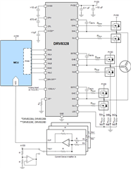
To implement three external CSAs using DRV8328, it is recommended to follow the block diagram implementation in Figure 1.
Figure 1 – DRV8328 using 3x external CSAs
Drawbacks of using a 3-shunt architecture with DRV8328
Because DRV8328 is designed for a 1-shunt external CSA architecture, there are drawbacks to implementing a 3-shunt external CSA architecture using Figure 1.
The main consideration is to tie LSS pin to the bottoms of the 3x external shunt resistors so that each motor phase has its own motor current path to accurately sense the current through the shunt without affecting the LSS sink current path for each low-side MOSFET gate driver output (GLx). However, this now ties the LSS pin to GND, which affects VDS overcurrent protection for the low-side MOSFET and VSEN overcurrent protection.
VDS overcurrent protection is set through the VDSLVL analog pin voltage. For the high-side MOSFET, the VDS overcurrent is measured from PVDD-SHx, so the VDSLVL value is calculated through the following equation: IOC = VDSLVL / RDS(ON). For the low-side MOSFET, the VDS overcurrent is measured from SHx to LSS (which in this case is tied to GND), so the resistor RSENSE adds to the total path resistance. This means the low-side MOSFET overcurrent value is calculated through the following equation: IOC = VDSLVL / (RDS(ON) + RSENSE).
For instance, if VDSLVL = 1V, RDS(ON) = 5mΩ, and RSENSE = 1mΩ, then Table 1 shows overcurrent thresholds will be detected across the high-side and low-side MOSFETs:
Table 1 – Example overcurrent threshold calculation when using 3 external CSA architecture
|
|
High-side MOSFET (PVDD-SHx) |
Low-side MOSFET (SHx-LSS) |
|
VDSLVL = 1V RDS(ON) = 5mΩ RSENSE = 1mΩ |
IOC = VDSLVL / RDS(ON) IOC = 1.0V / 0.005Ω IOC = 200 A |
IOC = VDSLVL / (RDS(ON) + RSENSE) IOC = 1.0V / (0.005+0.001)Ω IOC = 166.6 A |
VSEN overcurrent protection trips if the LSS-GND voltage > 0.5V. Because LSS tied to GND, VSEN overcurrent protection will never trip and is essentially disabled.
