This thread has been locked.

If you have a related question, please click the "Ask a related question" button in the top right corner. The newly created question will be automatically linked to this question.

DRV8300: On the U/V/W three-phase, when the low-side MOS transistor is turned on, Vgs has a large return channel. Is it because the driving capacity is insufficient?

Part Number: DRV8300
Other Parts Discussed in Thread: CSD88539ND

Hi Team,

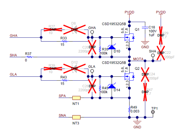
As shown in the figure below, csd88539nd is used for the MOS tube;

Schematic reference: DEMO_MD030A(001)_Sch;

The motor is a 13W BLDC motor, is this because of its insufficient drive capability? What improvement could I make?

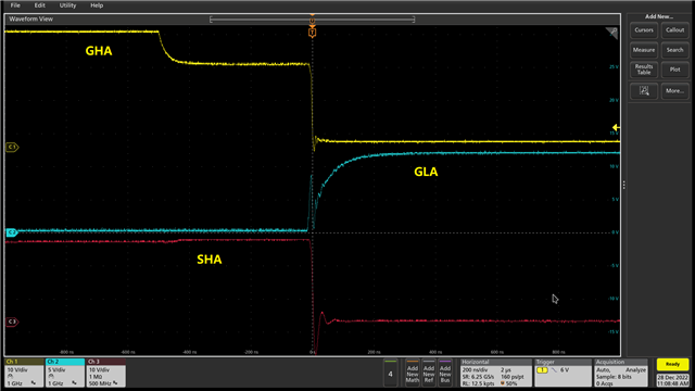
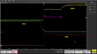
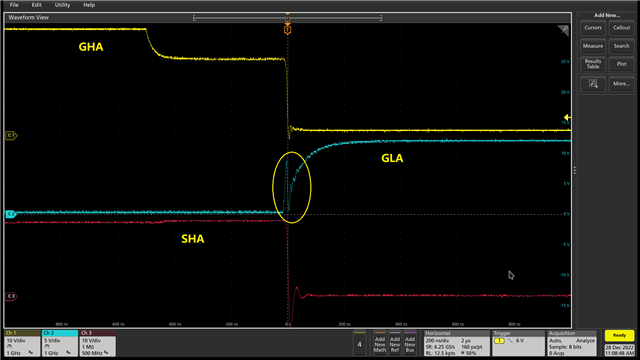
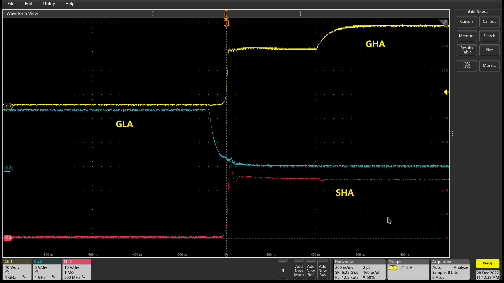
This is the VGS waveform generated when the upper tube MOS is turned on. It has a long plateau period.

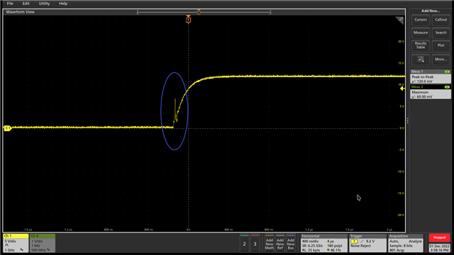
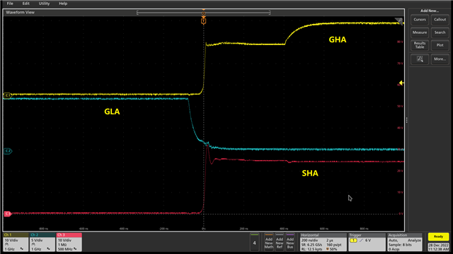
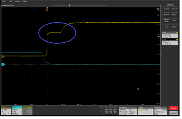
This is the VGS waveform generated when the lower tube MOS is turned on. It can only be opened with a large return channel.

Kind regards,

Katherine

  • Hi Katherine,

    It can only be opened with a large return channel.

    What can be opened, and what do you mean a large return channel?

    It is better to show the waveforms of both VGS and SHx in order to see the cause and effect of these signals. 

    Brian

  • Hi Brian,

    Sorry for the confusion.

    It can only be opened with a large return channel.

    The lower tube MOS can only be opened when there is a large ring-back.

    Kind regards,

    Katherine

  • Hi Brian,

    The waveforms of GHA/GLA and SHA are as follows.

    Regards,

    Katherine

  • Hi Katherine,

    Thank you for your question! The reason you are seeing the plateau is because you are measuring the GHx voltage with respect to ground. In order to determine if the high side MOSFET is on you need to look at the GHx voltage with respect to the SHx voltage. What you can see during the plateau is that the GHx voltage is the same voltage as the SHx voltage, which indicates that the high side FET is still off. The high side FET doesn't turn on until the end of the plateau, where you see the GHx voltage rise 10V above the SHx voltage. This "plateau" region is actually the deadtime between the low side MOSFET turning off and the high side MOSFET turning on. This dead time where both MOSFETs are off prevents shoot through from occurring.

    The reason the SHx voltage rises when GLx goes low is because the current is flowing into the phase when the low side MOSFET is turning off, and this current still must continue to flow. The current will flow through the body diode of the high side MOSFET, pulling the SHx voltage to VDRAIN. 

    There is a lot of voltage overshoot and undershoot that is occurring on SHx during switching. I would recommend reducing the gate drive current by increasing the gate resistance to slow down the SHx switching speed to minimize the overshoot and undershoot on SHx. We typically recommend a SHx slew rate of about 200ns rise time and 100ns fall time or slower.

    Regards,

    Anthony Lodi

  • Hi Katherine,

    The lower tube MOS can only be opened when there is a large ring-back.

    Do you mean MOS FET opened is the same as FET turned off? "ring-back" means voltage over shoot?

    The deadtime seems to be too long based on the scope waveforms. What is the deadtime and what connected to the DT pin on the chip?

    Suggestion: to help analyzing the waveform better, all signals should have their 0v level referenced to the scope grid line (line up the signal 0v on the grid line) as this makes the signal voltage measurement easier. 

    It has a long plateau period

    Because the deadtime is programmed to have a long value. By studying the signal waveforms of GHx, GLx, and SHx, you should continue to reduce the deadtime, as small as possible but not causing shoot-through (both FETs are turned on same time).

    Brian

  • Hi Brian,

    Do you mean MOS FET opened is the same as FET turned off? "ring-back" means voltage over shoot?

    The "ring-back" I mentioned means that the rising edge of the GLA signal of the lower tube has a relatively large drop, and then it rises again to fully open the lower tube, as shown in the figure below;

    Is this large rising edge derived from insufficient driving ability?

    Regards and thanks,

    Katherine

  • Hi Katherine,

    That drop on GLA is actually because the driving ability is too high. The high gate current is resulting in an extremely fast SHx switching speed (only a few nanoseconds slew rate). This is resulting in severe negative transients on SHx due to parasitic inductance on the PCB, which then makes GLA dip down as well. You should use a larger gate resistor to slow down the switching speed of the MOSFETs to reduce this ringing. That should solve your problem.

    Regards,

    Anthony Lodi

  • Is this large rising edge derived from insufficient driving ability?

    I might have the answer for this, but I'm waiting for your answer on my previous question as below:

    "What is the deadtime and what connected to the DT pin on the chip?"

    Brian

  • Hi Brian, 

    The customer replied that DRV used 20PIN DRV8300DPW and there was no DT pin.

    Regards,

    Katherine

  • Hi Katherine,

    The DRV8300DPW has a fixed deadtime, but additional deadtime can be added from the MCU if desired. Please see my previous responses and let me know if the customer has any additional questions after reading my replies. The main thing is increasing the gate resistance to slow down the switching speed of the MOSFETs to reduce the large inductive spiking that is occurring during switching.

    Regards,

    Anthony Lodi

  • Hi Anthony,

    The high side FET doesn't turn on until the end of the plateau, where you see the GHx voltage rise 10V above the SHx voltage. This "plateau" region is actually the deadtime between the low side MOSFET turning off and the high side MOSFET turning on.

    Katherine said the driver is a fixed deadtime with 200ns, so why the waveform below shows the deadtime is longer than 400ns, based on the plateau (200ns/division)?

    Brian

  • Hi Katherine,

    The customer replied that DRV used 20PIN DRV8300DPW and there was no DT pin.

    This driver has a fixed 200ns deadtime, but the waveform shows more than 400ns deadtime, so this makes no sense. Can you post the waveform of all these signals together so we can see the timing relationship from INLA and INHA to GLA and GHA and SHA?

    Brian

  • Hi Brian,

    I am not positive on why the deadtime is around 400ns, but looking at the INHx and INLx inputs will help to understand if there is some MCU deadtime being added. 

    Regards,

    Anthony Lodi

  • Hi Brian and Anthony,

    Thank you for your replies. The customer clicked at 'This resolved my issue' and his issue was settled.

    Thanks and regards,

    Katherine

  • Hi Katherine,

    Great to hear! 

    Regards

    Anthony Lodi