This thread has been locked.

If you have a related question, please click the "Ask a related question" button in the top right corner. The newly created question will be automatically linked to this question.

DRV8311HEVM: LDO output issue

Part Number: DRV8311HEVM

Hi team,

Here's an issue from the customer may need your help:

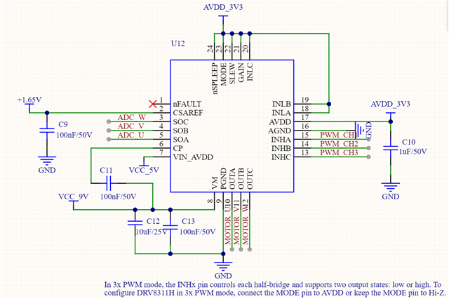
Using a driver designed with the DRV8311H, the current issues are as follows:

The LDO does not output 3.3 V. Is there any problem with the circuit design? (please see the schematic below)  Also, the nfault pin is floating, will this have any impact on the issue?

Pin 17 (AVDD) is the LDO inside the chip and should theoretically output 3.3V after power up. 

Could you help check this case? Thanks.

Best Regards,

Cherry

  • Hi Cherry,

    thanks for the question! What voltage is the customer measuring at the AVDD pin? What voltage is the customer measuring at the Vin AVDD pin during this time?

    Regards,

    Anthony

  • Hi Anthony,

    Thank you for your generous response! The voltage of the VIN_AVDD is 4.88V, and AVDD's voltage to GND is 0V (not even a little redundant, and I measured and found that AVDD is not shorted with GND).

    Regards,

    Sean

  • Hi Anthony.

    Thanks for your support. Sean is the customer I mentioned above and you could discuss on this issue directly, if any assistance needed please feel free to let me know.

    Thanks and regards,

    Cherry

  • Hi Anthony.

    I wonder if there is anything wrong with the schematic I designed like this?

    Thanks and regards,

    Sean

  • Hi Shen,

    The issue is that the AVDD_3V3 is connected directly to nSLEEP. nSLEEP needs to be high in order for the device to come out of sleep mode and for the AVDD LDO to be active. the AVDD LDO is disabled when nSLEEP is low (to reduce power consumption). nSLEEP needs to be high for the AVDD to output 3.3V, and AVDD needs to output 3.3V in order for nSLEEP to be high. this results in the device never powering up out of sleep mode.

    nSLEEP will need to be pulled high using a supply other than AVDD to work properly. 

    A few other notes: nFAULT needs to be pulled up to AVDD through a 5.1kohm pullup resistor. nFAULT is an open drain pin, so a pullup is required. Additionally, you may consider adding an output RC filter on the SOx outputs in case output filtering is needed.

    Regards,

    Anthony Lodi

  • Hi Anthony.,

    Thank you for your answer!I will modify the circuit as you suggested.

    Regards,

    Sean

  • Great! Sounds good.

    Regards,

    Anthony