Other Parts Discussed in Thread: DRV8353
Hi Friends,
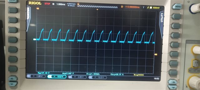
1. INHA,INLA,INHB,INLB,INHC and INLC six pwm is on gate high side and low side is perfect waveform.
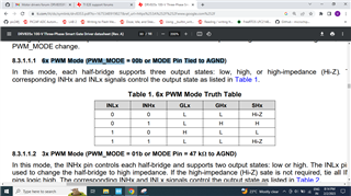
2. INHA,INHB,INHC ON and INLA,INLB,INLC OFF the low side is no pwm but high side gate wave is starting with 10v .
GHA,GHB,GHC high side gate wavefom below:

GLA,GLB,GLC Low side waveform below:
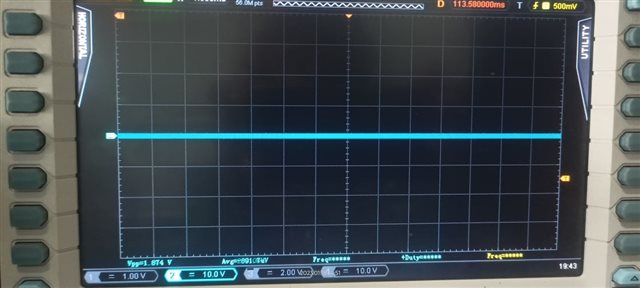
3.INHA,INHB,INHC OFF and INLA,INLB,INLC ON the low side pwm is correct but high side pwm is coming why reason .
GHA,GHB,GHC high side gate wavefom below:
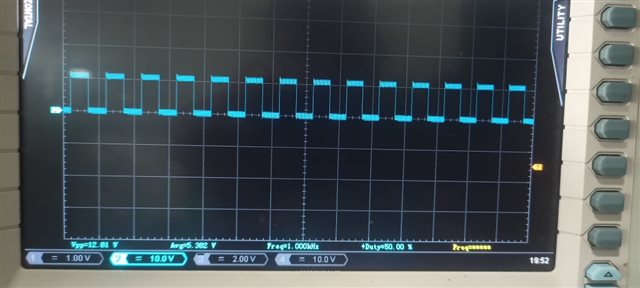
GLA,GLB,GLC Low side waveform below:
4. 120 degree phase shift wave form is not identify i upload low side gate and high side gate wave form
5. drv8353rs is default value
register 2 =0x0000
register 3 =0x03FF
register 4 =0x07FF
register 5 =0x016D
register 6 =0x0283
register 7 =0x0000
any register value are change tell meee.
5. drv8353rs high side gate waveform upload and low side gate waveform upload mee
Thanks Regards,
VJ.Pandi