This thread has been locked.

If you have a related question, please click the "Ask a related question" button in the top right corner. The newly created question will be automatically linked to this question.

DRV8323: Charge pump not activating

Part Number: DRV8323

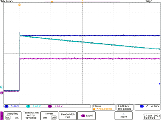
I'm having trouble getting the DRV8323H to start up and operate correctly.  The nFault line goes low within 6us of activating the Enable input.  Is there a particular timing sequence that needs to be applied to the chip to get it running?  


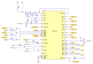
Some measurements that I took from the chip: 
VM (Pin 4) is ~28V
VDRAIN (Pin 5) is ~28V
VCP (Pin 3) capacitively discharges to 0V
DVDD (Pin 33) is ~4V
nFault (Pin 25) is 0V within 6us of Enable going high
Enable (Pin 30) is 3.3V
INLC (Pin 39) is 3.3V

  • Hi Rob,

    Thank you for posting to the Motor Drivers forum!

    To clarify, as you are starting up the device and monitoring the voltage on the VCP pin, you mention that the VCP discharges to 0V? Would you be able to share a waveform monitoring the voltage of the VCP pin as the nFault pin goes low?

    At the moment, it sounds like you are experiencing a VCP Charge Pump Undervoltage Lockout (CPUV) (refer to section 8.3.6.2 VCP Charge Pump Undervoltage Lockout (CPUV) for more details) and the waveform will help to confirm this. 

    Best,

    ~Alicia

  • Hi Alicia,

    I would agree that the charge pump isn't working.  Here is a scope capture of the chip on startup. 

    Channel 1 is VM

    Channel 2 is VCP

    Channel 3 is nFault (For some reason it is high until Enable is switched to 3.3V - it is currently low)

    I believe that VCP is discharging through the scope probe.  

    Is there a trick to getting the Charge Pump to start up? 

    Thanks,

    Rob

  • Hi Rob,

    There are a few reasons why you could be experiencing a charge pump undervoltage (CPUV):

    • The charge pump storage capacitor could be placed too far away from the device, has too large of a current loop, is too small in  capacitance, or has capacitance derating due to temperature or voltage bias
    • Gate driver outputs are demanding more average gate drive current than the current capability of the device’s charge pump
    • There is too much external load current on the charge pump if it is being used to drive an external load, such as a supply cutoff switch MOSFET

    More information about how to debug CPUV can be found on the following FAQs:

    Best,

    ~Alicia

  • Hi Rob,

    Please click the resolve button to let us know if this issue has been resolved.

    Closing the thread for now.

    Best,

    ~Alicia