This thread has been locked.

If you have a related question, please click the "Ask a related question" button in the top right corner. The newly created question will be automatically linked to this question.

DRV8873-Q1: Question about DRV8873-Q1 drive current

Part Number: DRV8873-Q1
Other Parts Discussed in Thread: DRV8262-Q1, DRV8244-Q1, DRV8243-Q1, DRV8245-Q1, DRV8245H-Q1EVM, DRV8262

Hello experts.

The current project wants to use the DRV8873-Q1 to drive a full-bridge brushed DC motor. The input voltage is 24V and the current is 5A. The ambient temperature is -40℃~85℃, can the DRV8873-Q1 meet the requirements?I'm having some difficulty calculating the junction temperature rise because calculating the temperature rise according to 5A would exceed the maximum junction temperature. How do I calculate this? Thanks.

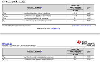
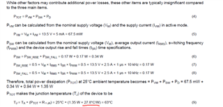
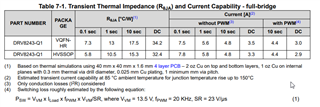
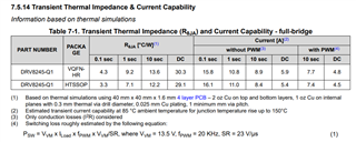
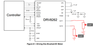
How do I calculate the junction temperature rise TJ at 85°C with a current of 5A, following the method of power calculation in the above diagram?

  • Hi,

    Thank you for your question. 

    Is customer looking for automotive 24V VBAT? If yes, normally customer require 65V abs max. Please check this with customer. We have 65V abs max device - DRV8262-Q1.

    If 65V is requirement, could you contact me internally to know customer opportunity in details? 

    If 40V abs max is good enough, I suggest DRV8243/44/45-Q1 family in stead of DRV8873-Q1. They are new gen of DRV8873-Q1.  DRV8243-Q1 is OK 5A a few second without PWM. DRV8244-Q1 can drive higher current than DRV8243-Q1.

    regards

    Shinya Morita

  • Hi,Shinya.

    Thank you for your response.

    Currently the product is used in commercial vehicles power supply is DC 18~32V, to drive 5A load, you can use the full-bridge drive can also use two half-bridge high side drive resistive load. It is planned to use DRV8245-Q1, because according to the calculation of junction temperature rise in the manual, DRV8245-Q1 can meet the requirement of 5A.

    There are a couple of questions that I hope will be answered.

    1、As shown above, the meaning in the comment is not clear, as the power supply used may be 32V, and if it is higher than 28V in the OUT shorted to ground it will not provide overcurrent protection?

    2、As shown above, the HW model is not supported for use in standalone mode how is the high resistance state of a single half-bridge to be interpreted? Does it mean that the OUT port of a single half-bridge cannot realize the high-resistance state?

    3、DRV824x_DRV814x-Q1EVM is it possible to provide the schematic and PCB LAYOUT?I didn't find the related technical information on the official website.

    4、The above figure shows that nFAULT,SPI(Opt),DRVOFF,nSLEEP, these signals suggest that they can be shared, does it mean that these signals from different chips can be controlled by category using one IO? For example, DRVOFF of chip A and DRVOFF of chip B can be controlled by one IO? But nFAULT is an OD gate, how can I tell which chip has an exception if they are combined together?

  • Hey Sheng,

    I will let Morita-san address 1 and 2.  

    3. See the Design Files section of the DRV8245H-Q1EVM page and download DRV82xxQ1EVM Hardware Files (Rev. A).  The schematic and PCB layout are then in the Sources subfolder with the Altium project. 

    4. Yes, just like you describe it.  For nFAULT you would not be able to tell which had the exception if they are combined together without some extra circuitry or steps.  If using a SPI version of the device you could check each device FAULT registers any time nFAULT signal changes, and by reading the registers could determine which device had an issue.  Or you could have a system logic where if any driver has a fault, stop and perform reset or something.  

    Regards,

    Jacob

  • Hi,

    If input voltage is DC up to 32V, I believe. Customer do not accept 40V abs max device like DRV8245-Q1.  We may need to recommend DRV8262-Q1 (65V abs max).

    I suggest to confirm this point first.

    regards

    Shinya Morita

  • Hi,Shinya.

    Voltage should indeed be considered. Choose a chip model with a higher input voltage.

    My usage requirement is that I need a single full-bridge drive output, but it should support 5A current, and the single full-bridge should support two independent half-bridge drives, because in addition to connecting to a motor, I may need to connect to some resistive loads. I checked the datasheet of DRV8262, it can support independent half-bridge drive mode? As shown in the diagram below. Two independent loads load1 and load2 can be connected externally and each of them can be driven with 5A current at 100% duty cycle. Can this scheme be realized?

  • Hi Sheng,

    Thank you for sharing your use case. 

    DRV8262-Q1 does not have independent mode. However PWM mode can be used for your 2x low side resistive load.

    By using bellow table, 4.9A DC (100% with OUT1 and OUT2 as low side resistive load) is OK. 8.4A up to 10sec. May need to increase PCB size a little more if you need 5A DC instead of 4.9A.

    regards

    Shinya Morita

  • Hi,Shinya.

    Do integrated MOS solutions have a chip with high voltage similar to the DRV8245-Q1 function?Does TI have a standalone controller externally driven MOS tube solution for my needs?

    What is the difference between the output signals on IN1/1N3 and IN2/IN4 for the PH/EN and PWM interfaces of the DRV8262, where PH/EN is a high and low level signal and PWM is an output pulse signal? What is the difference between these two?

    How do I set up DECAY and DECAY if I use the DRV8262 for my functional requirements?I don't understand the function of DECAY and TOFF.

  • Hi Sheng,

    With limitation of automotive products with high voltage 65V abs max FET integrated, DRV8262-Q1 is only product we can propose.

    Please refer bellow table in Datasheet. It shows the difference between PH/EN and PWM.

    In normal operation, DECAY mode can be referred above table. So not complicated.

    tOFF and Figure 7-5 is related to current regulation only. If you use current regulation/ITIRP function, need to care tOFF and Figure 7-5.

    regards

    Shinya Morita