This thread has been locked.

If you have a related question, please click the "Ask a related question" button in the top right corner. The newly created question will be automatically linked to this question.

DRV8323: SPI motor driver reports only "fault" and the fault pin is active

Part Number: DRV8323
Other Parts Discussed in Thread: CSD88599Q5DC

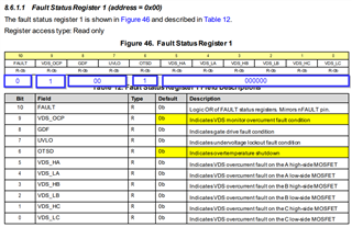
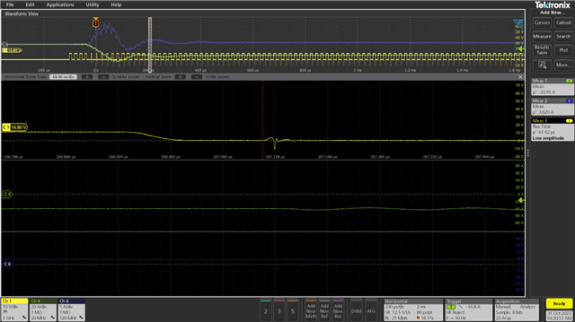
We've had a couple motor drivers stop functioning with the state as reported in the thread title. It gives no other debugging information (no other bits are set in either of the fault registers). From probing it appears that logic and other supplies are ok. I imagine that we've done something to damage the IC, I'm wondering if anyone is aware of the scenario that might help us further debug the cause that would lead to this state.

  • Upon more debugging I do on one see that that the charge pump voltage is low (VM + 0.384V). And I'm guessing this is maybe because vgls is low. It seems it should be able to report a charge pump undervoltage. Maybe it can't without Vgls? All the other SPI seems to work. What is a likely scenario to burn is this way? Overvoltage, undervoltage?

    SPI results:

    address: 2, reg_out: 1000, reg_in: 0
    address: 3, reg_out: 1bff, reg_in: 3ff
    address: 4, reg_out: 237f, reg_in: 37f
    address: 5, reg_out: 2804, reg_in: 4
    address: 6, reg_out: 3240, reg_in: 240
    drv8323s configure success
    drv8323 disabled, status1: 400 status2: 000

  • Hi Lee,

    I'm trying to get a better under standing of your problem. Can you clarify what you mean by address?


    address: 2,

    is this referring to control register 0x02?

    and what do you mean by reg_out and reg_in? is this what you are writing/reading via SPI? When writing or reading a register there should be 10 bits.

    Regards,

    Yara

  • You are correct. I added those extra printouts to show my configuration. Address 2 is the driver control register. I'm printing out the address and the 10 bit setting, which for register 2 is 0. It shows that SPI configuration is going through fine and that I'm not disabling the charge pump fault. So the current result of status register 1, which is address 0, is 0x400, which just indicates fault, but there is no other traceability to a source.

  • Hi Lee,

    Thank you for clarifying your process!

    A few things to mention

    1.

    I'm still a little confused and correct me if I am wrong but is your code printing out the SPI register bits in Hexadecimal or Decimal? Either way, some of these wouldn't translate to 10 bits

    address: 2, reg_out: 1000, reg_in: 0
    address: 3, reg_out: 1bff, reg_in: 3ff
    address: 4, reg_out: 237f, reg_in: 37f
    address: 5, reg_out: 2804, reg_in: 4
    address: 6, reg_out: 3240, reg_in: 240

    for example 1bff would be 0001101111111111 in binary, 16 bits, but it looks like you're only reading out 10 bits which would make sense because the device only knows how to read/write 10 bits. Make sure you are writing to the SPI registers using 10 bits binary, you can have your code take in hex or decimal as long as you are converting it to binary before you write it to the register. Use the following example of control register 2 as an example.

    If I follow the settings I've selected and highlighted in Table 15 I would have to write the 10 bits you see in the blue squares to the register, 01010000000 in binary or 0x280 in hex (again you have to write in binary to the device).

    2. 

    To address how to debug using SPI fault register is simple if you were to read out and print the bits from the register in binary. Look at the following table of fault register 1. If I read Fault Register 1 (0x00) and what came back was 0100100000 in binary (0x120 in hex). Looking at the table I can see bit 9 and 6 are set to 1, meaning in this scenario I get the following faults "Indicates VDS monitor overcurrent fault condition" and "Indicates overtemperature shutdown"

    remember there are TWO fault registers, reading from both will be able to tell you a lot about what is going on.

    Ultimately I have a feeling you're running into a SPI communication error. Trying to write more than 10 bits to your SPI registers will have you configuring certain registers unpredictably.

    Let me know if any of this information helps

    Regards,

    Yara

  • I still think I'm happy with the spi reads and writes, I've been using this code for a few years now. My issue is with a small number of these devices that sometimes burnout in a state that drives the nfault pin low and reports only fault in the status registers. I'm wondering what the likely scenario is. A better printout of my settings looks like below.

    Set enable pin, wait 10 ms then:
    address: 2, write: 0x000, read: 0x000
    address: 3, write: 0x3ff, read: 0x3ff
    address: 4, write: 0x37f, read: 0x37f
    address: 5, write: 0x004, read: 0x004
    address: 6, write: 0x240, read: 0x240

    Notice that nfault pin is low then read:
    address: 0, read: 0x400
    address: 1, read: 0x000
  • Is there a reason you are operating at max IDRIVE? 

  • I'm using the CSD88599q5dc fets, which I really like. I don't see any reason not to switch as fast as they can. There is no ringing on the PWM waveform.

  • Hi Lee, 

    You typically wouldn't see ringing on your PWM waveform if you are experiencing issues with a maxed out IDRIVE, ringing would be present on SHx or SLx.

    The FET you've chosen is not equipped to be driven with a maxed out IDRIVE that is why you may be experiencing damaged chips.

    Here's an FAQ that'll help

    https://e2e.ti.com/support/motor-drivers-group/motor-drivers/f/motor-drivers-forum/796378/faq-selecting-the-best-idrive-setting-and-why-this-is-essential?tisearch=e2e-sitesearch&keymatch=idrive%252520faq#

    and an app note

    https://www.ti.com/lit/an/slva714d/slva714d.pdf

    Regards,

    Yara

  • This is sort of a different direction than my original question. I'm still wondering what causes the driver to get stuck in this fault only state.

    But on the driver strength that is an appreciated point and good faq/app note. By PWM I meant the SH signal. That generally looks fine. Looking at SL and GL do look a bit troublesome. There is significant undershoot on GL/SL when the high side fet turns on, until I bring the high side gate drive strength down to 80 mA. I'd rather have a little bit less switching losses though. Are there any solutions to this undershoot problem? Do you think negative voltages on GL would cause this failure of the driver IC?

    Yellow is GL at 1 A high side gate strength.


    Now at 80 mA.


  • Hi Lee,

    Give me sometime to look at these waveforms, I'll get back to you in 24 hours.

    Regards,

    Yara

  • Hi Lee,

    So the waveforms you've provided lead me to believe that maxing out IDRIVE is in fact causing issues in your system. The undershoot you are seeing is significant and will potentially damage the device as this is pushing GLx outside of the recommended ratings. There are ways to help minimize the noise you are seeing on GLx but the chances of completely eliminating that noise might not be possible without lowering IDRIVE.

    I'd say look into RC snubbers: https://e2e.ti.com/support/motor-drivers-group/motor-drivers/f/motor-drivers-forum/991693/faq-proper-rc-snubber-design-for-motor-drivers

    Regards,

    Yara