This thread has been locked.

If you have a related question, please click the "Ask a related question" button in the top right corner. The newly created question will be automatically linked to this question.

DRV8703-Q1: Internal circuitry between VM and VCP

Part Number: DRV8703-Q1
Other Parts Discussed in Thread: DRV8705-Q1, DRV8702-Q1

Hi team,

My customer uses DRV8703-Q1 in their project and now they met an issue, could you please help give some comments? Thanks!

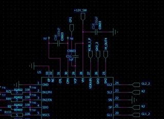
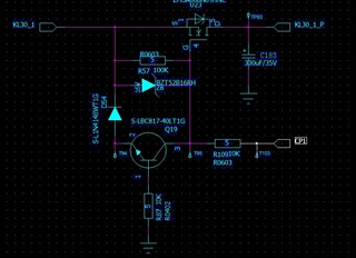
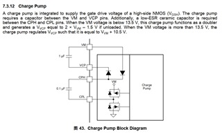
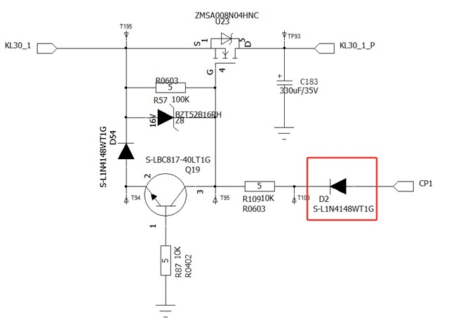
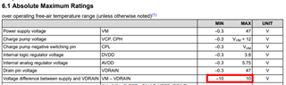
When the VCP is connected to Anti-Reverse Mos and the voltage is 10V and the VM is powered down, the measured voltage at the VM is 2V and the VGH is 0.

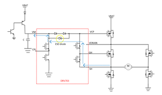
The voltage at the VM appears to be caused by leakage current inside the chip. However, according to the datasheet, there are two inverted diodes between the VM and the VCP, and the voltage on the VCP is theoretically not affecting the VM.

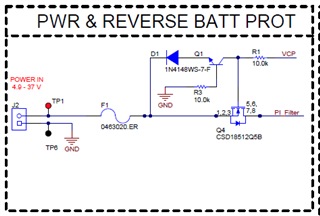
To avoid the effect of external capacitance, customer attempts to remove capacitance between VCP and VM, but there is still 2V at VM.

Could you please comments about the internal circuitry between VM and VCP? Since the VM has been powered down, is it possible that the voltage on the VCP can affect the VM's voltage through an internal circuit?

Thanks!

Regards,

Ivy

  • Hello Ivy, 

    Give me 24 hours to look into this and get back to you.

    Best,

    Keerthi

  • Hi Keerthi,

    Thanks! Add one more question.

    In order to avoid the problem of VMs still having 2V when the power off, which could cause excessive quiescent current, the customer wants to add a diode between the VCP and the anti-backflow circuit so that in sleep mode there is no voltage at the VCP. Do you think this is possible? And whether there is a potential risk. 

    Please give your suggestions. Thank you.

    Regards,

    Ivy

  • Hey Ivy,

    Thank you for the detailed information! Let me bring this to the attention of our automotive expert, he will respond early next week on this.  I have looked through and pulled up some relates posts [1] [2] but am not sure so need his help. 

    I would only recommend connecting one reverse-battery protection circuit per VCP since the charge pump can only drive small loads. The ultimate goal of reverse-battery protection is to cut the power to the board, so you only need the reverse battery protection at the power-entry point to the board.

    Best,

    Jacob

  • Hi Jacob,

    Thanks! Please help involve the expert to give suggestions on this case, many thanks!

    Regards,

    Ivy

  • Hi,

    Thank you for your questions. I guess your condition is KL30_1 = ~12V, but VM(+12V_SW) =0V. Is this correct?

    If yes, customer is probably violating abs max SPEC. This is not related to charge pump leakage current, but better to check.

    If customer would like to use different power supply for DRV's supply(VM) and FET's supply KL_30_1, I recommend to move to DRV8705-Q1. This device can support split supply.

    DRV8705Q1 EVM has example for reverse battery protection circuit by VCP. FYI.

    2577.MD023E3(005)_Sch.pdf

    regards

    Shinya Morita

  • Hi Morita,

    Thanks for your suggestions!

    But I still not sure the why the the measured voltage at the VM is 2V when power down, could you please share your comments on it?

    It seems like not related to the VM-VDRAIN abs max SPEC.

    Thanks!

    Regards,

    Ivy

  • Hi Morita,

    Thank you for your questions. why he VM-VDRAIN abs max SPEC is  ±10V?  Is there a 10V ESD  Zener diode  between VM-VDRAIN inside the IC?

  • Hello,

    Please give us another day to look into this.  Thanks!

  • Hi Morita,
    We applied a voltage of +14.4V between VM and VDRAIN,The measured current is 11.2mA.We applied a voltage of +14.4V between VDRAIN and VM,The measured current is 4.7μA.

    Thanks!
    Regards,
    bozhuo

  • Hi Morita,
    We applied a voltage of +14.4V between VM and VDRAIN,The measured current is 11.2mA.We applied a voltage of +14.4V between VDRAIN and VM,The measured current is 4.7μA.

    Thanks!
    Regards,
    bozhuo

  • Hi Bozhuo,

    Unfortunately, you are damaging DRV8703-Q1. VM-VDRAIN <10V is abs max condition. I have to suggest to replace potentially damaged part and stop doing this test.

    -If you connect VM and VDRAIN by changing schematic, DRV8703-Q1 should be fine. By adding D2 diode on VCP, I do not see the issue on DRV8703Q1 operation.

    -If customer would like to separate VM and VDRAIN and voltage gap could exceed 10V, I recommend move to DRV8705Q1.

    regards

    Shinya Morita

  • Hi Morita,
    why the VM-VDRAIN abs max SPEC is ±10V? If VDRAIN-VM>10V,Which part of the internal circuit is damaged?
    We understand that VM and VDRAIN are not related,Can you help demonstrate some VM-VDRAIN circuits.
    Thanks!
    Regards,
    bozhuo

  • Hi,

    Thank you for your question. We cannot disclose internal circuit, but I can say that DRV8702-Q1 has the circuit which has abs max 10V between VM and VDAIN. I have confirmed this SPEC is not against GND. 10V abs max is between VDRAIN and VM.

    regards

    Shinya Morita 

  • Hi Morita,

    We understand cannot disclose internal circuit,The product of this design is already on the market,We would like to assess the risks and Know the reason.

    why the VM-VDRAIN abs max SPEC is ±10V?

    Possible 1:

    if VM- VDRAIN>10V,Assyme VM=22v,VDRAIN=10V, VCP=VM+10.2V=32.2v,Turn on the external MOSFET,VGS=VCP-VDRAIN=20.2v>VGS(MOSFET) Maximum withstand voltage.


    if VM-VDRAIN<-10V,Assyme VM=12v,VDRAIN=22V, VCP=VM+10.2V=22.2v,Turn on the external MOSFET,VGS=VCP-VDRAIN=0.2v,It cannot open external MOSFET.


    Possible 2:

     This device cannot support split supply.Please see the picture(Our design),When ECU is in sleep mode,VM is powered down.If SH pin short to VBAT,It will damage ESD diode (10v Zener diode,Within the yellow circle).


    If possible 1,I think there is no risk,ECU is in work mode,VM is powered up.

    If Possible 2,I think there is low risk, SH pin not short to VBAT.

    Is there any other possibility? Can you help me analyze it?


    Thanks!
    Regards,
    bozhuo

  • Hi,

    Thank you for your questions. Although TI cannot share our internal circuit, let me ask a couple of questions to find solution.

    1) What is your position and background for these questions? (Your company is purchasing DRV to build ECU)?

    2) Is it possible to contact to TI sales person who support your company?

    3) Is your product under mass production with DRV8702-Q1 already? 

    4) Is "VM-VDRAIN >10V" happens during "DRV's Non-operation condition" only? For example, VM=0V and VDRAIN=~12V. Then nSLEELP is surely 0V when VDRAIN is >10V against VM.

    regards

    Shinya Morita

  • Hi Morita,

    Thank you for your answer.

    1) My company is purchasing DRV8703QRHBRQ1to build ECU.We are a Chinese company, and DRV8703Q is used for automobile seat control

    2) We have contacted TI's technical support.DRV8703-Q1: Internal circuitry between VM and VCP------ The  title was created by Ti's staff.

    3) The product is in the DV stage.We have already shipped over 1000 sets to the customer.

    4) Is "VM-VDRAIN >10V" happens during "DRV's Non-operation condition" only?    Yes

    For example, VM=0V and VDRAIN=~12V. Then nSLEELP is surely 0V when VDRAIN is >10V against VM.   Yes


    Thanks!
    Regards,
    bozhuo

  • Hi Bozhuo,

    Thank you for your reply. Based on your feedback, looks OK with your operation condition. Could you share TI contact person's name?

    regards

    Shinya Morita

  • Hi Bozhuo,

    Thanks. I will reach to Ivy Jin.

    regards

    Shinya Morita