Because of the holidays, TI E2E™ design support forum responses will be delayed from Dec. 25 through Jan. 2. Thank you for your patience.

This thread has been locked.

If you have a related question, please click the "Ask a related question" button in the top right corner. The newly created question will be automatically linked to this question.

DRV8718-Q1: Low-side current sense application

Part Number: DRV8718-Q1
Other Parts Discussed in Thread: DRV8705-Q1

Hi Shinya,

You had reviewed the schematic of DRV8718-Q1 on previous post below. There are additional questions on low-side current sense application. Please check it below and let me know.

https://e2e.ti.com/support/motor-drivers-group/motor-drivers/f/motor-drivers-forum/1253578/drv8718-q1-dual-power-supply-of-vbat

230822_SCH_feedback_DRV8718_low-side current sense.pdf

In this circuit we want to monitor the current using the low side concept. Is it correct to connect PGNDx to the + terminal of RSHUNT? We are currently evaluating the product after production, and it appears that there is an offset in the DRV8718 diagnostic function, so we would like to contact you to confirm.

Additionally, there is current sensing voltage interference between loads that commonly use PGND1 or PGND2, so we are reviewing the impact on the PGNDx connection point above and would like to request confirmation of the above information.

Regards,

  • Hello,

    Morita-san is currently out of office and will be back on Jan 4.

    Best,

    Keerthi

  • Hi Keerthi,

    Thanks for your response. Is there any person to support this case instead Shinya.

    Regards,

  • Hello Jeffrey,

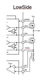
    Just to get some clarification on the question itself. I have looked at the previous post and the low side sense resistor seems to be in the right place. This is how low side sensing is configured:

    In your schematic:

    Is there an offset for loads that share Half bridges with different grounds. Is this what you mean? Can you also clarify by what you mean by this: there is an offset in the DRV8718 diagnostic function. What diagnostic function specifically and can you tell me the conditions in which it was measured.

    Best,

    Keerthi

  • Hi Keerthi,

    Please check an attached pdf file(Page 9 and 10) below that explains in more details.

    231228_SCH_feedback_DRV8718_R3.pptx

    Regards,

  • Hi Jeffrey,

    PGND1 should be connected to the system GND as outlined in the datasheet, but I am going to check with design on the actual purpose of this pin. Give me some time as most people are out of office right now. I will give an update mid next week.

    The following statement below is that before or after changing to the new configuration with PGND connected to GND:

    Best,

    Keerthi

  • Hi Keerthi,

    Shinya knows this case well, so please check it with Shinya and then let me know. Thanks for your support.

    Regards,

  • Hi Jeffrey,

    The reason why the PGNDx was recommended to be connected to the source of the FETs and the positive side of the sense resistor is to ensure that a false OCP condition doesn't happen due to the voltage across the shunt resistor. This is because the VDS sensing for LS FET is between PGND and SH. Is the current sensing voltage interference between loads observed on all the boards and have you tried this setup with an EVM. I will try on my end as well. I will also ask Morita-san once he is back in office.

    Best,

    Keerthi 

  • Hi Keerthi,

    Is there any update about this case?

    Regards,

  • Hi, 

    I just back to Office. Let me review the schematic and reply to you by tomorrow.

    regards

    Shinya Morita

  • Hi Jeffery,

    Thank you for your questions. PGND connection is a little complicated especally when customer use low side current sence.

    Here is summary

    1) PGND 1 and PGND 2 can be connected to system GND directly if current sense is high side or in-line or not used.

    2)With low side current sense, please use this way as I previously shared with you in previous post.PGND1 is for HB1-4, PNGD2 is for HB5-6.

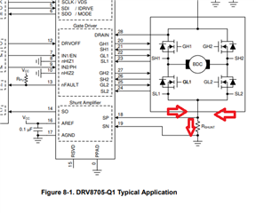
    We can refer DRV8705-Q1 Fig 8-1 as reference. This is example for low side current sense configuration. SLx pin of DRV8705-Q1 is same as PGNDx of DRV8718-Q1. We need to keep motor current flows to R_SHUNT with this configuration.

    Regarding offset, one suggestion for debug is to remove extra filter components(R,C) on SPx and SNx if they have. Noise filter R/C better to be added on SOx pin instead of SPx/SNx pin. 

    regards

    Shinya Morita

  • Hi Shinya,

    Thanks for your kind response. But there was additional question like page 9 and page 10 of attached file. Please check it and let me know.

    231228_SCH_feedback_DRV8718_R3.pptx

    Regards,

  • Hi Jeffrey,

    Thank you for your note. I did not noticed page 9 and 10 before. 

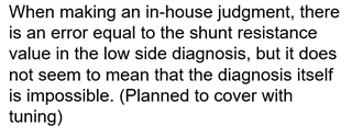
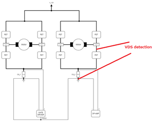
    I have reviewed page 9 and 10 then now I understand customer's issue situation. Bottom line is page 10 is only way customer can solve offset issue if customer need to use low side current sense for 2 HBs driving. Page 9 configuration could cause the offset issue.

    Then one key drawback of Page 10 solution is VDS detection at low side FET. Now VDS detection is monitoring voltage drop at "FET Rdson + CS_x(4mohm)". Please pay attention about this.

    regards

    Shinya Morita

  • Hi Shinya,

    One more question, please check #2 below of page 9 and let me know that.

    2. An error of more than 30% occurs in the current sensing part of the GATE DRIVER through 1mΩ. (The voltage across the shunt resistor is measured normally, but the VSO output has an error of about 30% in the calculated value - the error rate is maintained even when the load increases.)

    Ex) At 16.8A load, the voltage across the shunt is calculated as 0.0168V / VSO output voltage is calculated as 2.034V (offset not included), but when actually measured, the voltage across the shunt is almost the same / VSO output voltage is measured as 2.48V.)

    ※ Current sensing register settings are as follows.

    In the data sheet, there is only tolerance information for amplification and no information on output deviation, so please confirm whether there may be a 30% error.

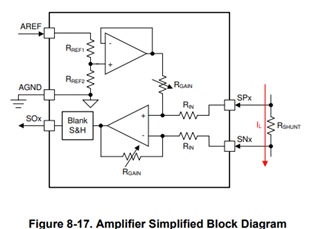
    For additional inquiries, please confirm whether your understanding of "Current Shunt Amplifier Configuration" is correct.

    When VAREF = 5V, VSO_BI = 2.25V / VSO_UNI = 4.125V.

    Can I think of the voltage value calculated here as the range that can be sensed?

    Example 1. When VSO_BI is set, the offset of VSO is approximately 2.5V. When inline sensing, current sensing can be used up to +2.25V when rising / -2.25V when falling based on 2.5V.

    Example 2. When VSO_UNI is set, the offset of VSO is approximately 0.7V. When sensing high side or low side, current sensing can be used up to 4.125V when rising from 0.7V.

    Is it correct to understand it as above?

    Regards,

  • Hi Jeffery.

    Thank you for your questions

    With original configuration, we can't measure motor current correctly on current sense amp. Error could be any value based on external sense resistance etc.

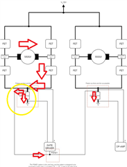
    Please refer bottom picture. All motor current on Left H-Bridge should go to current sense resister of left side. But with this connection, current will be split. Some portion goes to left sense resister, some some portion goes to right side sense resister. So sense output error value does not mean anything.

    regards

    Shinya Morita