


I'm seeing some behavior that I don't expect, and I want to know why the gate driver is doing this. It seems like IDRIVEP_HS isn't being applied when it should be.
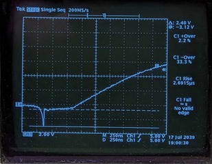
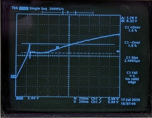
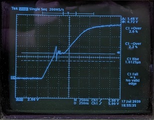
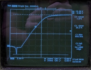
I have IDRIVE (all 4 of them) at 300 mA (IDRIVEP_HS = 4, IDRIVEN_HS = 3, IDRIVEP_LS = 4, IDRIVEN_LS = 3). TDRIVE is 3 (4000 ns) and DEAD_TIME is 1 (100 ns) The gate voltage waveforms and rise and fall times are what I expect for 6 of the 8 gate edges, but the high side gate rise times are much slower. It almost seems that it's acting as if IDRIVEP_HS is closer to 50 mA - 100 mA in some situations. With current flowing out of the half bridge (high side gate rising is switching the half bridge), the current appears to be what I configured before and during the plateau, but seems too low afterwards. With current flowing into the half bridge (high side gate rising does not switch the half bridge), the current seems too low for the entire duration.
In both cases, the low current is during a time when power MOSFET is not actually switching, so this might be intentional, but it still seems strange. Is this what the DRV8350S should be doing?
Here's pictures of the 2 waveforms that seem wrong. They continue rising in a similar exponential decay curve until they hit 9.5V or so. The displayed measurements are over the entire scope capture buffer (which includes reaching the final voltage):
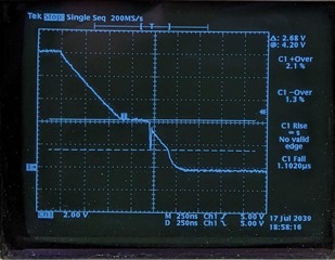
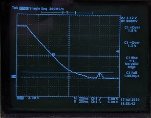
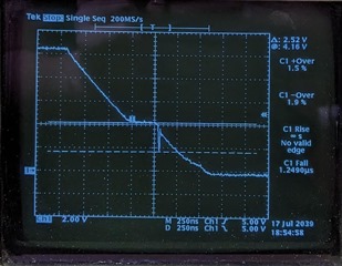
And here's the 2 high side falling waveforms (these look like I expect):
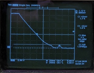
And here's the 4 low side waveforms (these also look like I expect):
All of these waveforms were captured at steady state with 150A on this phase (in either direction), and 75A on the other 2 phases (in the opposite direction). The same measurements on the other 2 phases look very similar with the 150A through them instead, the only difference I see is the amplitude of the ringing/transients is slightly lower on the phase that's closest to the gate driver.
My design uses 2 IPTG014N10NM5 in parallel (12 MOSFETs total for all 3 phases), each one has 169 nC nominal gate charge. I'm using FOC switching at 20 kHz (control loop runs at both midpoints of the PWM so the control loop is at 40 kHz), which is 20.3 mA I_VCP / I_VGLS, which is under the 25 mA rating.
I'm probing vias directly underneath the MOSFET pads with a ground clip. The probe is a 500 MHz 10x high-impedance passive probe. The scope is 500 MHz. High side measurements are with scope ground on the phase, the test setup is battery powered so it floats.


